SCDS447 July 2021 TMUX1248
PRODUCTION DATA
- 1 Features
- 2 Applications
- 3 Description
- 4 Revision History
- 5 Pin Configuration and Functions
-
6 Specifications
- 6.1 Absolute Maximum Ratings
- 6.2 ESD Ratings
- 6.3 Recommended Operating Conditions
- 6.4 Thermal Information
- 6.5 Electrical Characteristics (VDD = 5 V ±10 %), GND = 0 V unless otherwise specified.
- 6.6 Electrical Characteristics (VDD = 3.3 V ±10 %), GND = 0 V unless otherwise specified.
- 6.7 Electrical Characteristics (VDD = 1.8 V ±10 %), GND = 0 V unless otherwise specified.
- 6.8 Electrical Characteristics (VDD = 1.2 V ±10 %), GND = 0 V unless otherwise specified.
- 6.9 Typical Characteristics
- 7 Parameter Measurement Information
- 8 Detailed Description
- 9 Power Supply Recommendations
- 10Layout
- 11Device and Documentation Support
- 12Mechanical, Packaging, and Orderable Information
Package Options
Mechanical Data (Package|Pins)
- DCK|6
Thermal pad, mechanical data (Package|Pins)
Orderable Information
3 Description
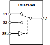
The TMUX1248 is a general purpose 2:1, single-pole double-throw (SPDT), switch that supports a wide operating range of 1.08 V to 5.5 V. The device supports bidirectional analog and digital signals on the source (Sx) and drain (D) pins ranging from GND to VDD. The state of the select pin (SEL) controls which of the two sources pins are connected to the drain pin. Additionally, the TMUX1248 has a low supply current of 7 nA which enables the device to be used in a host of handheld or low power applications.
Break-before-make switching prevents both source pins from being enabled simultaneously. This feature adds robustness in the system by preventing source signals from shorting during switching events.
All logic inputs have 1.8 V logic compatible thresholds, allowing for operation with low voltage logic signals. Fail-Safe Logic circuitry allows voltages on the control pins to be applied before the supply pin, or at a higher voltage than the supply pin up to 5.5 V, protecting the device from potential damage.
| PART NUMBER | PACKAGE | BODY SIZE (NOM) |
|---|---|---|
| TMUX1248 | SC70 (6) | 2.00 mm × 1.25 mm |
 TMUX1248 Block Diagram
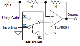
 Application Example