SCDS426E March 2020 – October 2022 TMUX1308 , TMUX1309
PRODUCTION DATA
- 1 Features
- 2 Applications
- 3 Description
- 4 Revision History
- 5 Device Comparison Table
- 6 Pin Configuration and Functions
-
7 Specifications
- 7.1 Absolute Maximum Ratings
- 7.2 ESD Ratings
- 7.3 Recommended Operating Conditions
- 7.4 Thermal Information: TMUX1308
- 7.5 Thermal Information: TMUX1309
- 7.6 Electrical Characteristics
- 7.7 Logic and Dynamic Characteristics
- 7.8 Timing Characteristics
- 7.9 Injection Current Coupling
- 7.10 Typical Characteristics
- 8 Parameter Measurement Information
-
9 Detailed Description
- 9.1 Overview
- 9.2 Functional Block Diagram
- 9.3
Feature Description
- 9.3.1 Bidirectional Operation
- 9.3.2 Rail-to-Rail Operation
- 9.3.3 1.8 V Logic Compatible Inputs
- 9.3.4 Fail-Safe Logic
- 9.3.5
Injection Current Control
- 9.3.5.1 TMUX13xx is Powered, Channel is Unselected, and the Input Signal is Greater Than VDD (VDD = 5 V, VINPUT = 5.5 V)
- 9.3.5.2 TMUX13xx is Powered, Channel is Selected, and the Input Signal is Greater Than VDD (VDD = 5 V, VINPUT = 5.5 V)
- 9.3.5.3 TMUX13xx is Unpowered and the Input Signal has a Voltage Present (VDD = 0 V, VINPUT = 3 V)
- 9.4 Device Functional Modes
- 9.5 Truth Tables
- 10Application and Implementation
- 11Power Supply Recommendations
- 12Layout
- 13Device and Documentation Support
- 14Mechanical, Packaging, and Orderable Information
Package Options
Mechanical Data (Package|Pins)
Thermal pad, mechanical data (Package|Pins)
- BQB|16
Orderable Information
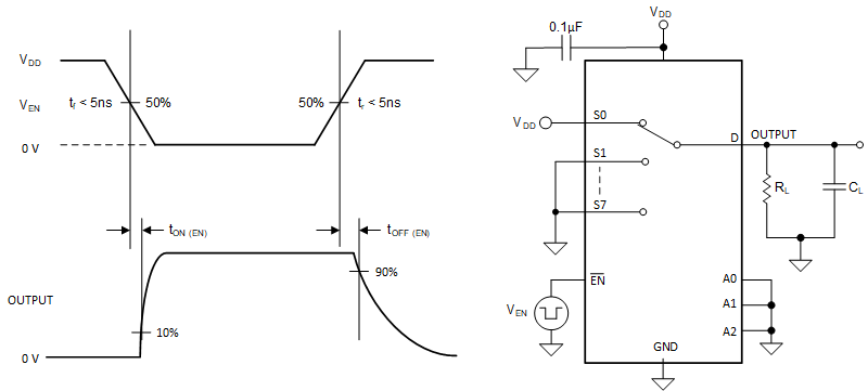
8.6 tON(EN) and tOFF(EN)
Turn-on time is defined as the time taken by the output of the device to rise to 10% after the enable has risen past the 50% threshold. The 10% measurement is utilized to provide the timing of the device, system level timing can then account for the time constant added from the load resistance and load capacitance. Figure 8-6 shows the setup used to measure transition time, denoted by the symbol tON(EN).
Turn-off time is defined as the time taken by the output of the device to fall to 90% after the enable has fallen past the 50% threshold. The 90% measurement is utilized to provide the timing of the device, system level timing can then account for the time constant added from the load resistance and load capacitance. Figure 8-6 shows the setup used to measure transition time, denoted by the symbol tOFF(EN).
 Figure 8-6 Turn-On and Turn-Off Time Measurement Setup