SCDS367E august   2017  – june 2023 TMUX136

PRODUCTION DATA  

  1.   1
  2. Features
  3. Applications
  4. Description
  5. Revision History
  6. Pin Configuration and Functions
  7. Specifications
    1. 6.1 Absolute Maximum Ratings
    2. 6.2 ESD Ratings
    3. 6.3 Recommended Operating Conditions
    4. 6.4 Thermal Information
    5. 6.5 Electrical Characteristics
    6. 6.6 Dynamic Characteristics
    7. 6.7 Timing Requirements
    8. 6.8 Typical Characteristics
  8. Parameter Measurement Information
  9. Detailed Description
    1. 8.1 Overview
    2. 8.2 Functional Block Diagram
    3. 8.3 Feature Description
      1. 8.3.1 Low Power Mode
    4. 8.4 Device Functional Modes
      1. 8.4.1 High Impedance Mode
  10. Application and Implementation
    1. 9.1 Application Information
    2. 9.2 Typical Application
      1. 9.2.1 Design Requirements
      2. 9.2.2 Detailed Design Procedure
      3. 9.2.3 Application Curves
    3. 9.3 Power Supply Recommendations
    4. 9.4 Layout
      1. 9.4.1 Layout Guidelines
      2. 9.4.2 Layout Example
  11. 10Device and Documentation Support
    1. 10.1 Documentation Support
      1. 10.1.1 Related Documentation
    2. 10.2 Receiving Notification of Documentation Updates
    3. 10.3 Support Resources
    4. 10.4 Trademarks
    5. 10.5 Electrostatic Discharge Caution
    6. 10.6 Glossary
  12. 11Mechanical, Packaging, and Orderable Information

Package Options

Refer to the PDF data sheet for device specific package drawings

Mechanical Data (Package|Pins)
  • RSE|10
Thermal pad, mechanical data (Package|Pins)
Orderable Information

Application Curves

GUID-7A30D4C8-3EB3-40C7-85F7-FB0707D30669-low.gif
Figure 9-2 Eye Pattern: 0.7 Gbps with No Device
GUID-CE8DF26F-8F87-42F3-B254-7ED53FFBD04A-low.gif
The TMUX136 contributes only 8.4 ps of peak-to-peak jitter for 0.7-Gbps data rate
Figure 9-4 Eye Pattern: 0.7 Gbps with Switch
GUID-F2EA4BA8-16A3-493C-B931-2AEFEE9BC013-low.gif
Figure 9-6 Eye Pattern: 2.2 Gbps with No Device
GUID-97BFE415-879C-450D-8E85-B1149899A98B-low.gif
The TMUX136 contributes only 3.8 ps of peak-to-peak jitter for 2.2-Gbps data rate
Figure 9-8 Eye Pattern: 2.2 Gbps with Switch
GUID-524B513F-4D1A-47E1-BE4D-9DA624F13FB9-low.gif
Figure 9-10 Eye Pattern: 3 Gbps with No Device
GUID-1FA5B49A-2402-491C-BC76-4ABDA2E0005D-low.gif
The TMUX136 contributes only 5.8 ps of peak-to-peak jitter for 3-Gbps data rate
Figure 9-12 Eye Pattern: 3 Gbps with Switch
GUID-789233B3-0735-465F-A967-FA3322C663FD-low.gif
Figure 9-14 Eye Pattern: 4.5 Gbps with No Device
GUID-7C72EE7B-37E1-4316-B274-A511BD9E0963-low.gif
The TMUX136 contributes only 7.6 ps of peak-to-peak jitter for 4.5-Gbps data rate
Figure 9-16 Eye Pattern: 4.5 Gbps with Switch
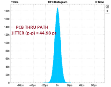
GUID-42D592BD-918C-4123-87D8-F84E15756E1F-low.gifFigure 9-3 Time Interval Error Histogram: 0.7 Gbps with No Device
GUID-5D797273-C0D9-485F-8654-5F680DE159E9-low.gif
The TMUX136 contributes only 8.4 ps of peak-to-peak jitter for 0.7-Gbps data rate
Figure 9-5 Time Interval Error Histogram: 0.7 Gbps with Switch
GUID-893A9E61-49ED-4D91-A92C-472341510731-low.gifFigure 9-7 Time Interval Error Histogram: 2.2 Gbps with No Device
GUID-9A555D68-B041-478D-A995-AF7AF1E50334-low.gif
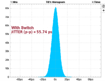
The TMUX136 contributes only 3.8 ps of peak-to-peak jitter for 2.2-Gbps data rate
Figure 9-9 Time Interval Error Histogram: 2.2 Gbps with Switch
GUID-99621967-D4B2-4CCB-9761-18D73EF118BC-low.gifFigure 9-11 Time Interval Error Histogram: 3 Gbps with No Device
GUID-7477963E-EBA4-433C-B362-1AE6BE923205-low.gif
The TMUX136 contributes only 5.8 ps of peak-to-peak jitter for 3-Gbps data rate
Figure 9-13 Time Interval Error Histogram: 3 Gbps with Switch
GUID-61D472E4-DEB8-48AC-B459-F2D3D7DAB886-low.gif
Figure 9-15 Time Interval Error Histogram: 4.5 Gbps with No Device
GUID-D73451A4-85B9-455F-AE8B-B479C20EF1C1-low.gif
The TMUX136 contributes only 7.6 ps of peak-to-peak jitter for 4.5-Gbps data rate
Figure 9-17 Time Interval Error Histogram: 4.5 Gbps with Switch