SCDS423A October   2020  – May 2024 TMUX1575

PRODUCTION DATA  

  1.   1
  2. Features
  3. Applications
  4. Description
  5. Pin Configuration and Functions
    1.     Pin Functions
  6. Specifications
    1. 5.1 Absolute Maximum Ratings
    2. 5.2 ESD Ratings
    3. 5.3 Recommended Operating Conditions
    4. 5.4 Thermal Information
    5. 5.5 Electrical Characteristics
    6. 5.6 Dynamic Characteristics
    7. 5.7 Timing Requirements
    8. 5.8 Typical Characteristics
  7. Parameter Measurement Information
    1. 6.1  On-Resistance
    2. 6.2  Off-Leakage Current
    3. 6.3  On-Leakage Current
    4. 6.4  IPOFF Leakage Current
    5. 6.5  Transition Time
    6. 6.6  tON (EN) and tOFF (EN) Time
    7. 6.7  Break-Before-Make Delay
    8. 6.8  Charge Injection
    9. 6.9  Off Isolation
    10. 6.10 Channel-to-Channel Crosstalk
    11. 6.11 Bandwidth
  8. Detailed Description
    1. 7.1 Overview
    2. 7.2 Functional Block Diagram
    3. 7.3 Feature Description
      1. 7.3.1 Bidirectional Operation
      2. 7.3.2 Beyond Supply Operation
      3. 7.3.3 1.2V Logic Compatible Inputs
      4. 7.3.4 Powered-off Protection
      5. 7.3.5 Fail-Safe Logic
      6. 7.3.6 Integrated Pull-Down Resistors
    4. 7.4 Device Functional Modes
      1. 7.4.1 Truth Tables
  9. Application and Implementation
    1. 8.1 Typical Application
      1. 8.1.1 Design Requirements
      2. 8.1.2 Detailed Design Procedure
    2. 8.2 Power Supply Recommendations
    3. 8.3 Layout
      1. 8.3.1 Layout Guidelines
      2. 8.3.2 Layout Example
  10. Device and Documentation Support
    1. 9.1 Documentation Support
      1. 9.1.1 Related Documentation
    2. 9.2 Receiving Notification of Documentation Updates
    3. 9.3 Support Resources
    4. 9.4 Trademarks
    5. 9.5 Electrostatic Discharge Caution
    6. 9.6 Glossary
  11. 10Revision History
  12. 11Mechanical, Packaging, and Orderable Information
    1. 11.1 Mechanical Data

Package Options

Refer to the PDF data sheet for device specific package drawings

Mechanical Data (Package|Pins)
  • YCJ|16
Thermal pad, mechanical data (Package|Pins)
Orderable Information

Typical Characteristics

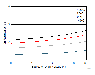
At TA = 25°C, VDD = 3.3V (unless otherwise noted).
TMUX1575 On-Resistance
            vs Temperature
VDD = 3.3V
Figure 5-1 On-Resistance vs Temperature
TMUX1575 On-Resistance
            vs Source or Drain Voltage
TA = 25°C
Figure 5-3 On-Resistance vs Source or Drain Voltage
TMUX1575 Supply Current
            vs Logic Voltage
TA = 25°C
Figure 5-5 Supply Current vs Logic Voltage
TMUX1575 TON
              (EN) vs Supply Voltage
TA = 25°C
Figure 5-7 TON (EN) vs Supply Voltage
TMUX1575 Skew and
            Propagation Delay vs Supply Voltage
TA = 25°C
Figure 5-9 Skew and Propagation Delay vs Supply Voltage
TMUX1575 On-Response vs
            Frequency
TA = 25°C
Figure 5-11 On-Response vs Frequency
TMUX1575 On-Resistance
            vs Temperature
VDD = 1.8V
Figure 5-2 On-Resistance vs Temperature
TMUX1575 On-Leakage vs
           Source or Drain Voltage
VDD = 3.3V
Figure 5-4 On-Leakage vs Source or Drain Voltage
TMUX1575 TTRANSITION vs Supply Voltage
TA = 25°C
Figure 5-6 TTRANSITION vs Supply Voltage
TMUX1575 TOFF
              (EN) vs Supply Voltage
TA = 25°C
Figure 5-8 TOFF (EN) vs Supply Voltage
TMUX1575 Off Isolation
            and Crosstalk vs Frequency
TA = 25°C
Figure 5-10 Off Isolation and Crosstalk vs Frequency