SCDS464B June 2023 – July 2024 TMUX2889
PRODUCTION DATA
- 1
- 1 Features
- 2 Applications
- 3 Description
- 4 Pin Configuration and Functions
- 5 Specifications
-
6 Parameter Measurement Information
- 6.1 On-Resistance
- 6.2 On-Leakage Current
- 6.3 Off-Leakage Current
- 6.4 Power-Off Leakage Current
- 6.5 tON (VDD) and tOFF (VDD) Time
- 6.6 Transition Time
- 6.7 Break-Before-Make
- 6.8 Propagation Delay
- 6.9 THD + Noise
- 6.10 Power Supply Rejection Ratio (PSRR)
- 6.11 Charge Injection
- 6.12 Bandwidth
- 6.13 Off Isolation
- 6.14 Crosstalk
- 7 Detailed Description
- 8 Application and Implementation
- 9 Device and Documentation Support
- 10Revision History
- 11Mechanical, Packaging, and Orderable Information
Package Options
Refer to the PDF data sheet for device specific package drawings
Mechanical Data (Package|Pins)
- YBH|9
Thermal pad, mechanical data (Package|Pins)
Orderable Information
6.1 On-Resistance
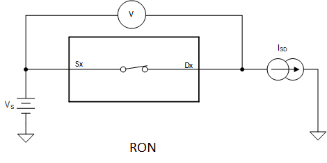
The on-resistance of a device is the ohmic resistance between the source (Sx) and drain (Dx) pins of the device. The on-resistance varies with input voltage and supply voltage. The symbol RON is used to denote on-resistance. Figure 6-1 shows the measurement setup used to measure RON. Voltage (V) and current (ISD) are measured using this setup, and RON is computed with RON = V / ISD.
 Figure 6-1 On-Resistance
Measurement Setup