SCDS419E November 2020 – July 2024 TMUX6208 , TMUX6209
PRODUCTION DATA
- 1
- 1 Features
- 2 Applications
- 3 Description
- 4 Device Comparison Table
- 5 Pin Configuration and Functions
-
6 Specifications
- 6.1 Absolute Maximum Ratings
- 6.2 ESD Ratings
- 6.3 Thermal Information
- 6.4 Recommended Operating Conditions
- 6.5 Source or Drain Continuous Current
- 6.6 ±15 V Dual Supply: Electrical Characteristics
- 6.7 ±15 V Dual Supply: Switching Characteristics
- 6.8 36 V Single Supply: Electrical Characteristics
- 6.9 36 V Single Supply: Switching Characteristics
- 6.10 12 V Single Supply: Electrical Characteristics
- 6.11 12 V Single Supply: Switching Characteristics
- 6.12 ±5 V Dual Supply: Electrical Characteristics
- 6.13 ±5 V Dual Supply: Switching Characteristics
- 6.14 Typical Characteristics
-
7 Parameter Measurement Information
- 7.1 On-Resistance
- 7.2 Off-Leakage Current
- 7.3 On-Leakage Current
- 7.4 Transition Time
- 7.5 tON(EN) and tOFF(EN)
- 7.6 Break-Before-Make
- 7.7 tON (VDD) Time
- 7.8 Propagation Delay
- 7.9 Charge Injection
- 7.10 Off Isolation
- 7.11 Crosstalk
- 7.12 Bandwidth
- 7.13 THD + Noise
- 7.14 Power Supply Rejection Ratio (PSRR)
- 8 Detailed Description
- 9 Application and Implementation
- 10Device and Documentation Support
- 11Revision History
- 12Mechanical, Packaging, and Orderable Information
Package Options
Mechanical Data (Package|Pins)
Thermal pad, mechanical data (Package|Pins)
- RUM|16
Orderable Information
3 Description
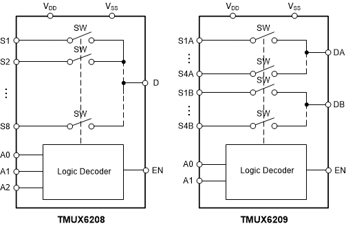
The TMUX6208 is a precision 8:1, single channel multiplexer while the TMUX6209 is a 4:1, 2 channel multiplexer featuring low on resistance and charge injection. The devices work with a single supply (4.5V to 36V), dual supply (±4.5V to ±18V), or asymmetric supply (such as VDD = 12V, VSS = –5V). The TMUX620x supports bidirectional analog and digital signals onthe source (Sx) and drain (D) pins ranging from VSS to VDD.
All logic control inputs support logic high levels from 1.8 V to VDD, ensuring both TTL and CMOS logic compatibility when operating in the valid supply voltage range. Fail-Safe Logic circuitry allows voltages on the control pins to be applied before the supply pin, protecting the device from potential damage.
The TMUX620x are part of the precision switches and multiplexers family of devices. These devices have very low on and off leakage currents and low charge injection, allowing them to be used in high precision measurement applications.
| PART NUMBER | CONFIGURATION | PACKAGE (1) |
|---|---|---|
| TMUX6208 | 1 Channel 8:1 Multiplexer | TSSOP (16) (PW) WQFN (16) (RUM) |
| TMUX6209 | 2 Channel 4:1 Multiplexer |
 TMUX6208 and TMUX6209 Block Diagram