SCDS420E September 2020 – July 2024 TMUX6219
PRODUCTION DATA
- 1
- 1 Features
- 2 Applications
- 3 Description
- 4 Pin Configuration and Functions
-
5 Specifications
- 5.1 Absolute Maximum Ratings
- 5.2 ESD Ratings
- 5.3 Thermal Information
- 5.4 Recommended Operating Conditions
- 5.5 Source or Drain Continuous Current
- 5.6 ±15 V Dual Supply: Electrical Characteristics
- 5.7 ±15 V Dual Supply: Switching Characteristics
- 5.8 36 V Single Supply: Electrical Characteristics
- 5.9 36 V Single Supply: Switching Characteristics
- 5.10 12 V Single Supply: Electrical Characteristics
- 5.11 12 V Single Supply: Switching Characteristics
- 5.12 +5 V / -8 V Dual Supply: Electrical Characteristics
- 5.13 +5 V / -8 V Dual Supply: Switching Characteristics
- 5.14 ±5 V Dual Supply: Electrical Characteristics
- 5.15 ±5 V Dual Supply: Switching Characteristics
- 5.16 Typical Characteristics
-
6 Parameter Measurement Information
- 6.1 On-Resistance
- 6.2 Off-Leakage Current
- 6.3 On-Leakage Current
- 6.4 Transition Time
- 6.5 tON(EN) and tOFF(EN)
- 6.6 Break-Before-Make
- 6.7 tON (VDD) Time
- 6.8 Propagation Delay
- 6.9 Charge Injection
- 6.10 Off Isolation
- 6.11 Crosstalk
- 6.12 Bandwidth
- 6.13 THD + Noise
- 6.14 Power Supply Rejection Ratio (PSRR)
- 7 Detailed Description
- 8 Application and Implementation
- 9 Power Supply Recommendations
- 10Layout
- 11Device and Documentation Support
- 12Revision History
- 13Mechanical, Packaging, and Orderable Information
Package Options
Mechanical Data (Package|Pins)
Thermal pad, mechanical data (Package|Pins)
Orderable Information
6.3 On-Leakage Current
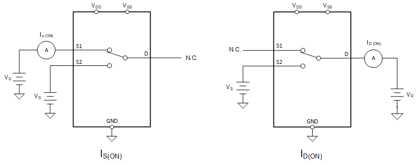
Source on-leakage current is defined as the leakage current flowing into or out of the source pin when the switch is on. This current is denoted by the symbol IS(ON).
Drain on-leakage current is defined as the leakage current flowing into or out of the drain pin when the switch is on. This current is denoted by the symbol ID(ON).
Either the source pin or drain pin is left floating during the measurement. Figure 6-3 shows the circuit used for measuring the on-leakage current, denoted by IS(ON) or ID(ON).
 Figure 6-3 On-Leakage Measurement Setup