-
TMUX6236 36V, Low-RON, 2:1 (SPDT), 2-Channel Precision Switch With 1.8V Logic
- 1
- 1 Features
- 2 Applications
- 3 Description
- 4 Pin Configuration and Functions
-
5 Specifications
- 5.1 Absolute Maximum Ratings
- 5.2 ESD Ratings
- 5.3 Thermal Information
- 5.4 Recommended Operating Conditions
- 5.5 Source or Drain Continuous Current
- 5.6 ±15V Dual Supply: Electrical Characteristics
- 5.7 ±15V Dual Supply: Switching Characteristics
- 5.8 36V Single Supply: Electrical Characteristics
- 5.9 36V Single Supply: Switching Characteristics
- 5.10 12V Single Supply: Electrical Characteristics
- 5.11 12V Single Supply: Switching Characteristics
- 5.12 ±5V Dual Supply: Electrical Characteristics
- 5.13 ±5V Dual Supply: Switching Characteristics
- 5.14 Typical Characteristics
-
6 Parameter Measurement Information
- 6.1 On-Resistance
- 6.2 Off-Leakage Current
- 6.3 On-Leakage Current
- 6.4 Transition Time
- 6.5 tON(EN) and tOFF(EN)
- 6.6 Break-Before-Make
- 6.7 tON (VDD) Time
- 6.8 Propagation Delay
- 6.9 Charge Injection
- 6.10 Off Isolation
- 6.11 Crosstalk
- 6.12 Bandwidth
- 6.13 THD + Noise
- 6.14 Power Supply Rejection Ratio (PSRR)
- 7 Detailed Description
- 8 Application and Implementation
- 9 Device and Documentation Support
- 10Revision History
- 11Mechanical, Packaging, and Orderable Information
- IMPORTANT NOTICE
Package Options
Refer to the PDF data sheet for device specific package drawings
Mechanical Data (Package|Pins)
- PW|16
- RUM|16
Thermal pad, mechanical data (Package|Pins)
- RUM|16
Orderable Information
TMUX6236 36V, Low-RON, 2:1 (SPDT), 2-Channel Precision Switch With 1.8V Logic
1 Features
- Dual supply range: ±4.5V to ±18V
- Single supply range: 4.5V to 36V
- Low on-resistance: 2Ω
- High current support: 330mA (maximum) (WQFN)
- –40°C to +125°C operating temperature
- 1.8V logic compatible
- Integrated pull-down resistor on logic pins
- Fail-safe logic
- Rail-to-rail operation
- Bidirectional operation
2 Applications
- Factory automation and industrial controls
- Programmable logic controllers (PLC)
- Analog input modules
- ATE test equipment
- Battery monitoring systems
- Ultrasound scanners
- Patient monitoring and diagnostics
- Optical networking
- Optical test equipment
- Remote radio units
- Wired networking
- Data acquisition systems
3 Description
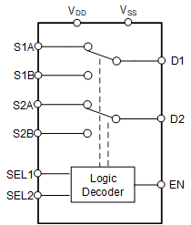
The TMUX6236 is a complementary metal-oxide semiconductor (CMOS) switch with two 2:1 switches. The device works well with dual supplies (±4.5V to ±18V), a single supply (4.5V to 36V), or asymmetric supplies (such as VDD = 12V, VSS = –5V). The TMUX6236 supports bidirectional analog and digital signals on the source (Sx) and drain (D) pins ranging from VSS to VDD.
All logic control inputs support logic levels from 1.8V to VDD, allowing for both TTL and CMOS logic compatibility when operating in the valid supply voltage range. Fail-Safe Logic circuitry allows voltages on the control pins to be applied before the supply pin, protecting the device from potential damage.
| PART NUMBER | PACKAGE(1) | PACKAGE SIZE(2) |
|---|---|---|
| TMUX6236 | RUM (WQFN, 16) | 4mm × 4mm |
| PW (TSSOP, 16) | 5mm × 6.4mm |
 Block Diagram
4 Pin Configuration and Functions
 Figure 4-1 RUM Package,16-Pin WQFN(Top View)
| PIN | TYPE(1) | DESCRIPTION | ||
|---|---|---|---|---|
| NAME | TSSOP | WQFN | ||
| D1 | 3 | 1 | I/O | Drain pin. Can be an input or output. |
| D2 | 11 | 9 | I/O | Drain pin. Can be an input or output. |
| EN | 14 | 12 | I | Active high logic enable, has internal pull-up resistor. When this pin is low, all switches are turned off. When this pin is high, the SEL logic input determine which switch is turned on. |
| GND | 6 | 4 | P | Ground (0V) reference |
| NC |
7, 8, 15, 16 |
5, 7, 13, 14 | — | No internal connection. Can be shorted to GND or left floating. |
| S1A |
2 |
16 | I/O | Source pin 1A. Can be an input or output. |
| S1B |
4 |
2 | I/O | Source pin 1B. Can be an input or output. |
| S2A | 10 |
8 | I/O | Source pin 2A. Can be an input or output. |
| S2B | 12 |
10 | I/O | Source pin 2B. Can be an input or output. |
| SEL1 | 1 | 15 | I | Logic control input, has internal pull-down resistor. Table 7-1 lists how to control the switch connection. |
| SEL2 | 9 | 6 | I | Logic control input, has internal pull-down resistor. Table 7-1 lists how to control the switch connection. |
| VDD | 13 | 11 | P | Positive power supply. This pin is the most positive power-supply potential. For reliable operation, connect a decoupling capacitor ranging from 0.1µF to 10µF between VDD and GND. |
| VSS | 5 | 3 | P | Negative power supply. This pin is the most negative power-supply potential. In single-supply applications, this pin can be connected to ground. For reliable operation, connect a decoupling capacitor ranging from 0.1µF to 10µF between VSS and GND. |
| Thermal Pad | — | The thermal pad is not connected internally. There is no requirement to electrically connect this pad. If connected, however, it is recommended that the pad be left floating or tied to GND. | ||