SCDS449C April 2022 – February 2024 TMUX6236
PRODUCTION DATA
- 1
- 1 Features
- 2 Applications
- 3 Description
- 4 Pin Configuration and Functions
-
5 Specifications
- 5.1 Absolute Maximum Ratings
- 5.2 ESD Ratings
- 5.3 Thermal Information
- 5.4 Recommended Operating Conditions
- 5.5 Source or Drain Continuous Current
- 5.6 ±15V Dual Supply: Electrical Characteristics
- 5.7 ±15V Dual Supply: Switching Characteristics
- 5.8 36V Single Supply: Electrical Characteristics
- 5.9 36V Single Supply: Switching Characteristics
- 5.10 12V Single Supply: Electrical Characteristics
- 5.11 12V Single Supply: Switching Characteristics
- 5.12 ±5V Dual Supply: Electrical Characteristics
- 5.13 ±5V Dual Supply: Switching Characteristics
- 5.14 Typical Characteristics
-
6 Parameter Measurement Information
- 6.1 On-Resistance
- 6.2 Off-Leakage Current
- 6.3 On-Leakage Current
- 6.4 Transition Time
- 6.5 tON(EN) and tOFF(EN)
- 6.6 Break-Before-Make
- 6.7 tON (VDD) Time
- 6.8 Propagation Delay
- 6.9 Charge Injection
- 6.10 Off Isolation
- 6.11 Crosstalk
- 6.12 Bandwidth
- 6.13 THD + Noise
- 6.14 Power Supply Rejection Ratio (PSRR)
- 7 Detailed Description
- 8 Application and Implementation
- 9 Device and Documentation Support
- 10Revision History
- 11Mechanical, Packaging, and Orderable Information
Package Options
Refer to the PDF data sheet for device specific package drawings
Mechanical Data (Package|Pins)
- PW|16
- RUM|16
Thermal pad, mechanical data (Package|Pins)
- RUM|16
Orderable Information
3 Description
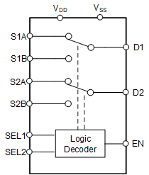
The TMUX6236 is a complementary metal-oxide semiconductor (CMOS) switch with two 2:1 switches. The device works well with dual supplies (±4.5V to ±18V), a single supply (4.5V to 36V), or asymmetric supplies (such as VDD = 12V, VSS = –5V). The TMUX6236 supports bidirectional analog and digital signals on the source (Sx) and drain (D) pins ranging from VSS to VDD.
All logic control inputs support logic levels from 1.8V to VDD, allowing for both TTL and CMOS logic compatibility when operating in the valid supply voltage range. Fail-Safe Logic circuitry allows voltages on the control pins to be applied before the supply pin, protecting the device from potential damage.
| PART NUMBER | PACKAGE(1) | PACKAGE SIZE(2) |
|---|---|---|
| TMUX6236 | RUM (WQFN, 16) | 4mm × 4mm |
| PW (TSSOP, 16) | 5mm × 6.4mm |
 Block Diagram