SCDS432 June 2021 TMUX646
PRODUCTION DATA
- 1 Features
- 2 Applications
- 3 Description
- 4 Revision History
- 5 Pin Configuration and Functions
- 6 Specifications
- 7 Parameter Measurement Information
- 8 Detailed Description
- 9 Application and Implementation
- 10Power Supply Recommendations
- 11Layout
- 12Device and Documentation Support
- 13Mechanical, Packaging, and Orderable Information
Package Options
Mechanical Data (Package|Pins)
- ZEC|36
Thermal pad, mechanical data (Package|Pins)
Orderable Information
9.2.2.2 MIPI C-PHY Application
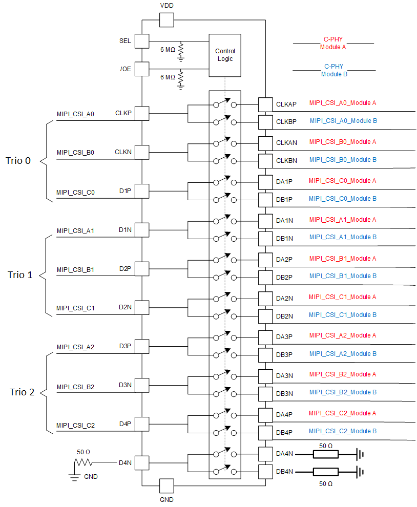
The clock and data lanes can be interchanged as necessary to facilitate the best layout possible for the application. In addition, the signal lines of the TMUX646 are routed single ended on the chip die. This makes the device suitable for differential and single-ended high-speed systems. This also allows the positive and negative lines to be interchanged as necessary to facilitate the best layout possible for the application.
C-PHY application includes 3 trios of signals, which may be routed on any channel, which means there will be one unused channel on the TMUX646. TI recommends that the unused I/O signal pin be connected to ground through a 50 Ω resistor to prevent signal reflections and maintain device performance.
 Figure 9-4 MIPI C-PHY Example Pinout