SCDS403C february 2021 – july 2023 TMUX7308F , TMUX7309F
PRODUCTION DATA
- 1
- 1 Features
- 2 Applications
- 3 Description
- 4 Revision History
- 5 Device Comparison Table
- 6 Pin Configuration and Functions
-
7 Specifications
- 7.1 Absolute Maximum Ratings
- 7.2 ESD Ratings
- 7.3 Thermal Information
- 7.4 Recommended Operating Conditions
- 7.5 Electrical Characteristics (Global)
- 7.6 ±15 V Dual Supply: Electrical Characteristics
- 7.7 ±20 V Dual Supply: Electrical Characteristics
- 7.8 12 V Single Supply: Electrical Characteristics
- 7.9 36 V Single Supply: Electrical Characteristics
- 7.10 Typical Characteristics
-
8 Parameter Measurement Information
- 8.1 On-Resistance
- 8.2 Off-Leakage Current
- 8.3 On-Leakage Current
- 8.4 Input and Output Leakage Current Under Overvoltage Fault
- 8.5 Break-Before-Make Delay
- 8.6 Enable Delay Time
- 8.7 Transition Time
- 8.8 Fault Response Time
- 8.9 Fault Recovery Time
- 8.10 Charge Injection
- 8.11 Off Isolation
- 8.12 Crosstalk
- 8.13 Bandwidth
- 8.14 THD + Noise
- 9 Detailed Description
- 10Application and Implementation
- 11Device and Documentation Support
- 12Mechanical, Packaging, and Orderable Information
Package Options
Mechanical Data (Package|Pins)
Thermal pad, mechanical data (Package|Pins)
Orderable Information
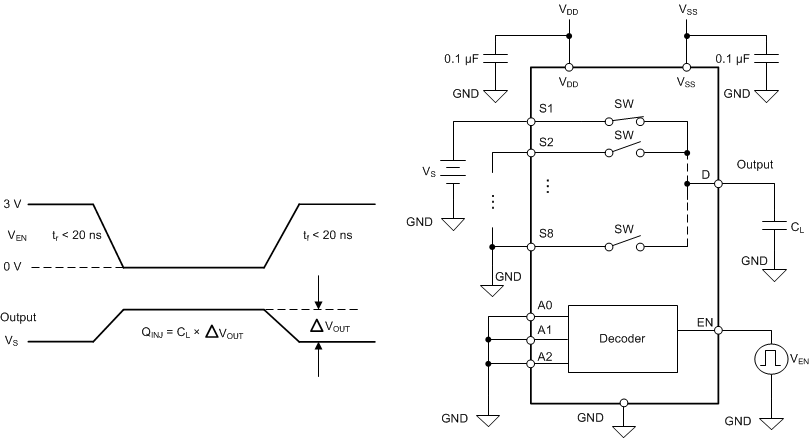
8.10 Charge Injection
Charge injection is a measure of the glitch impulse transferred from the logic input to the signal path during logic pin switching, and is denoted by the symbol QINJ. Figure 8-11 shows the setup used to measure charge injection from the source to drain.
 Figure 8-11 Charge-Injection Measurement Setup