SCDS466A August 2023 – December 2024 TMUX7612
PRODUCTION DATA
- 1
- 1 Features
- 2 Applications
- 3 Description
- 4 Pin Configuration and Functions
-
5 Specifications
- 5.1 Absolute Maximum Ratings
- 5.2 ESD Ratings
- 5.3 Thermal Information
- 5.4 Source or Drain Current through Switch
- 5.5 Recommended Operating Conditions
- 5.6 Electrical Characteristics (Global)
- 5.7 Electrical Characteristics (±15 V Dual Supply)
- 5.8 Switching Characteristics (±15 V Dual Supply)
- 5.9 Electrical Characteristics (±20 V Dual Supply)
- 5.10 Switching Characteristics (±20 V Dual Supply)
- 5.11 Electrical Characteristics (+37.5 V/–12.5 V Dual Supply)
- 5.12 Switching Characteristics (+37.5 V/–12.5 V Dual Supply)
- 5.13 Electrical Characteristics (12 V Single Supply)
- 5.14 Switching Characteristics (12 V Single Supply)
- 5.15 Typical Characteristics
- 6 Parameter Measurement Information
- 7 Detailed Description
- 8 Application and Implementation
- 9 Device and Documentation Support
- 10Revision History
- 11Mechanical, Packaging, and Orderable Information
Package Options
Mechanical Data (Package|Pins)
Thermal pad, mechanical data (Package|Pins)
- RUM|16
Orderable Information
6.10 THD + Noise
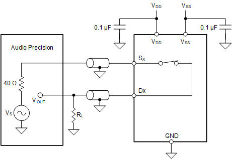
The total harmonic distortion (THD) of a signal is a measurement of the harmonic distortion, and is defined as the ratio of the sum of the powers of all harmonic components to the power of the fundamental frequency at the mux output. The on-resistance of the device varies with the amplitude of the input signal and results in distortion when the drain pin is connected to a low-impedance load. Total harmonic distortion plus noise is denoted as THD + N.
 Figure 6-10 THD + N
Measurement Setup