SLASEW5A December 2020 – October 2024 TMUXHS4412
PRODUCTION DATA
- 1
- 1 Features
- 2 Applications
- 3 Description
- 4 Pin Configuration and Functions
- 5 Specifications
- 6 Detailed Description
- 7 Application and Implementation
- 8 Device and Documentation Support
- 9 Revision History
- 10Mechanical, Packaging, and Orderable Information
Package Options
Mechanical Data (Package|Pins)
- RUA|42
Thermal pad, mechanical data (Package|Pins)
- RUA|42
Orderable Information
5.8 Typical Characteristics
The following figures show differential insertion loss on the top plot and return loss on the bottom plot of a typical TMUXHS4412 channel. Note measurements are performed in TI evaluation board with board and equipment parasitics calibrated out.
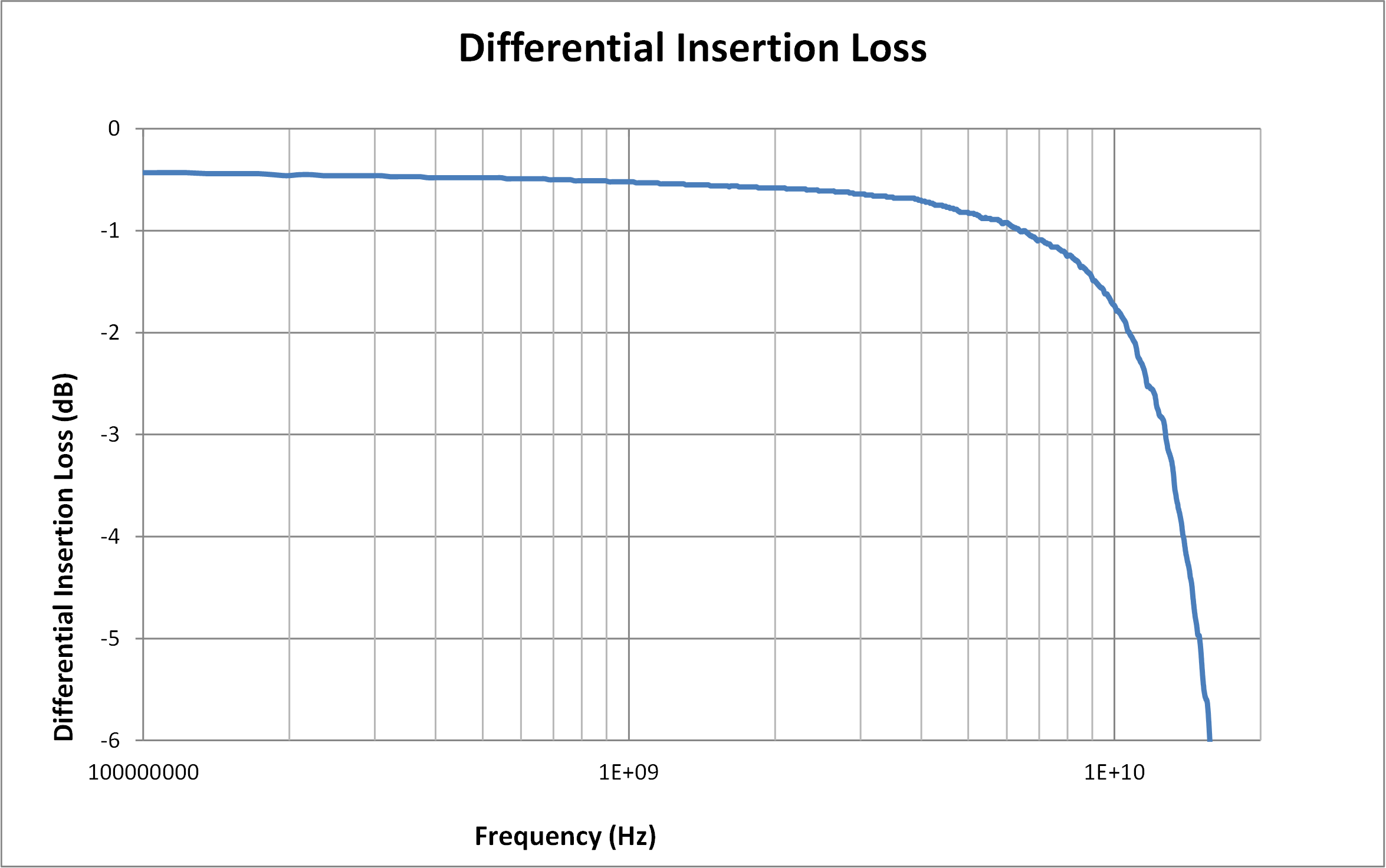
Figure 5-1 S-Parameter Plots for a TMUXHS4412 Channel: Differential Insertion Loss
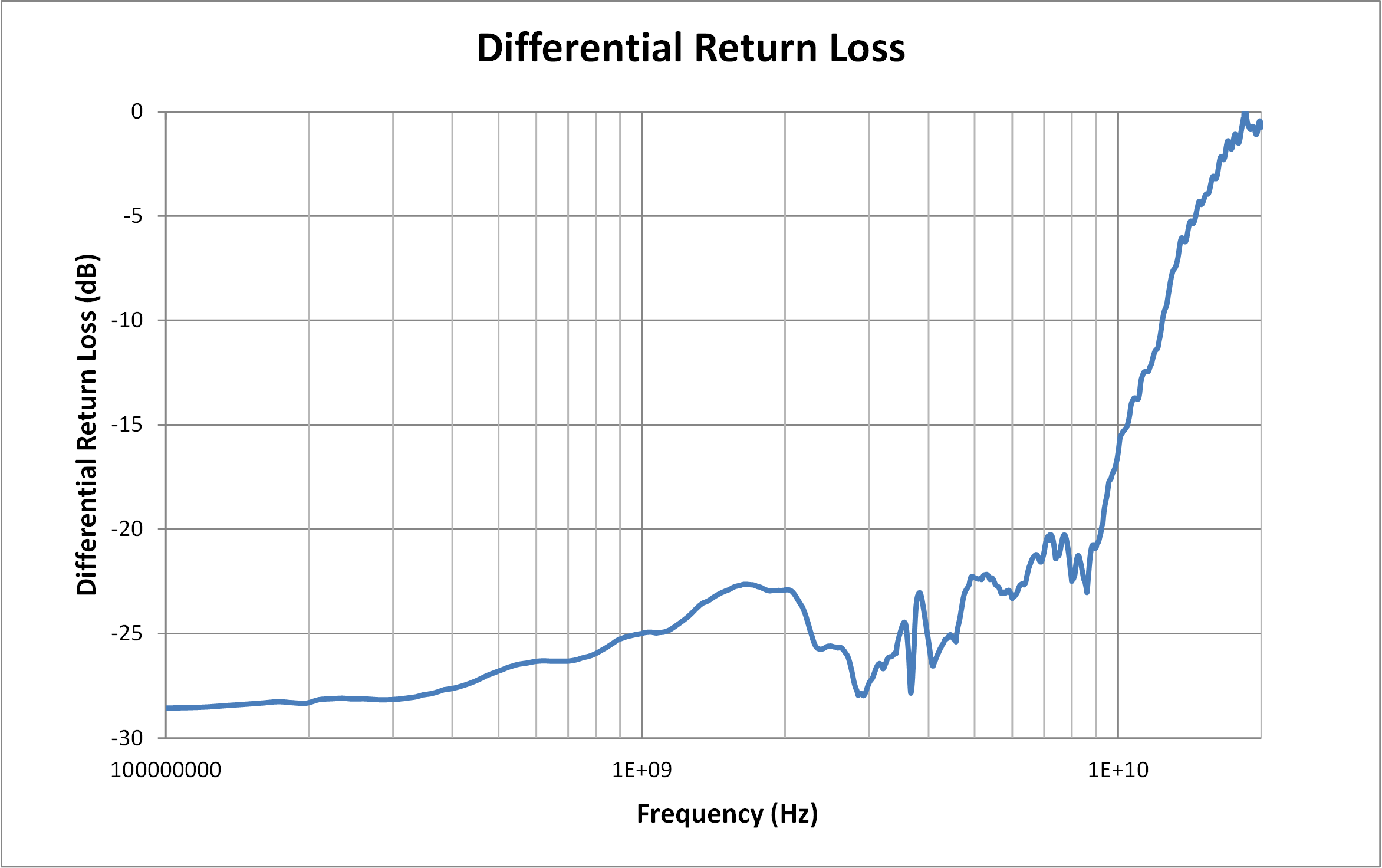
Figure 5-2 S-Parameter Plots for a TMUXHS4412 Channel: Return Loss vs Frequency
The following figures show side-by-side comparisons of 10Gbps signals through calibration traces and a typical TMUXHS4412 channels.
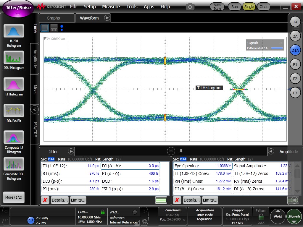 Figure 5-3 Jitter Decomposition of 10Gbps
PRBS-7 Signals in TI Evaluation Board Through Calibration Traces
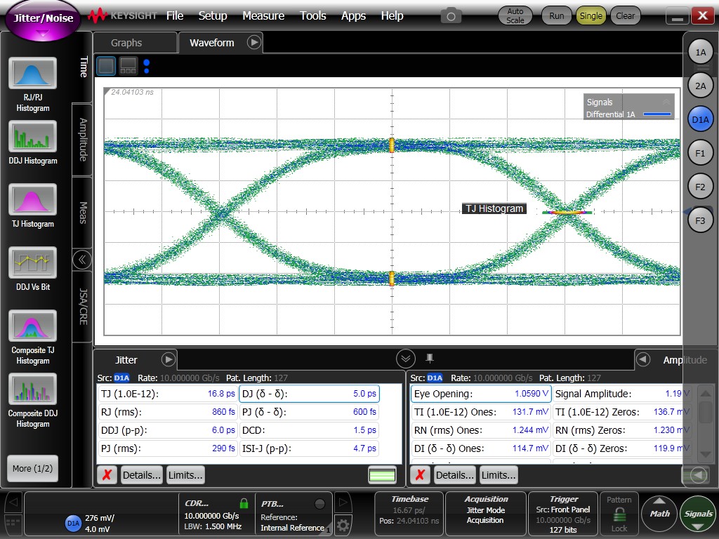 Figure 5-4 Jitter Decomposition of 10Gbps
PRBS-7 Signals in TI Evaluation Board Through a Typical TMUXHS4412 Channel
Figure 5-4 Jitter Decomposition of 10Gbps
PRBS-7 Signals in TI Evaluation Board Through a Typical TMUXHS4412 ChannelThe following figures show side-by-side comparisons of 20Gbps signals through calibration traces and a typical TMUXHS4412 channels.
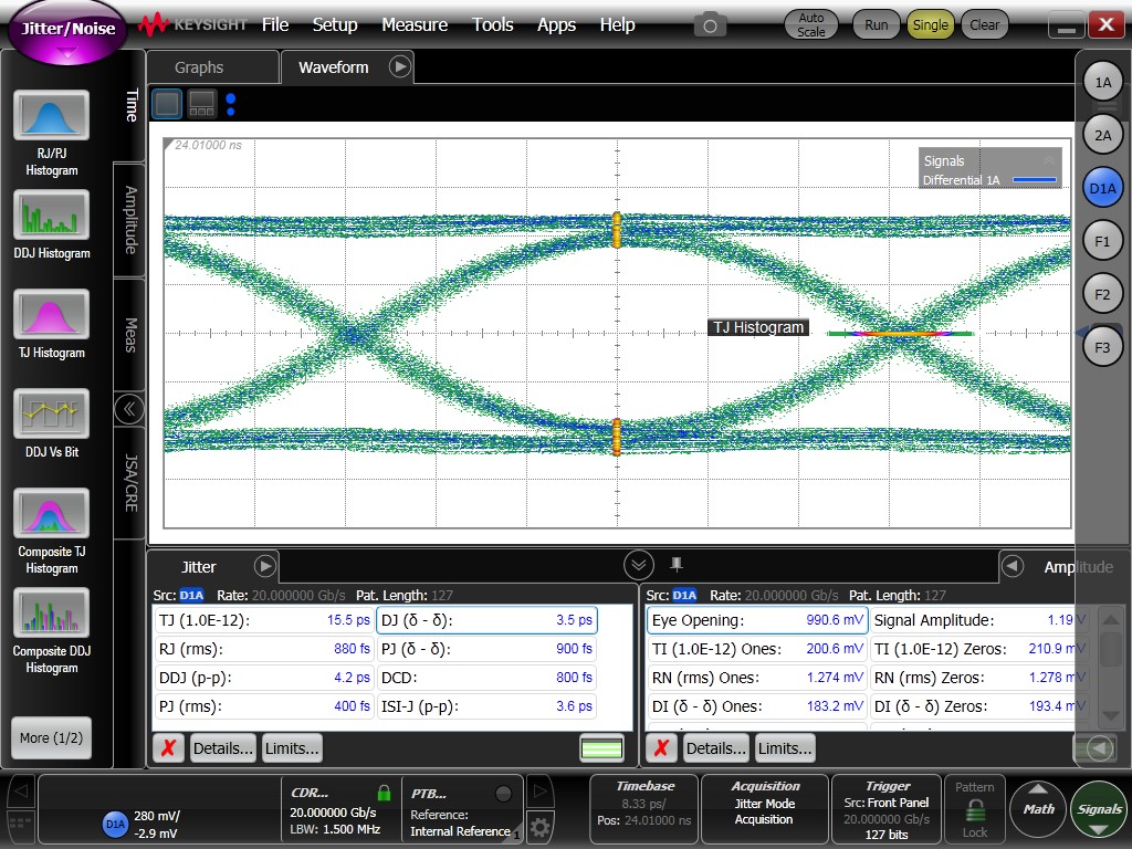 Figure 5-5 Jitter
Decomposition of 20Gbps PRBS-7 Signals in TI Evaluation Board Through Calibration Traces
 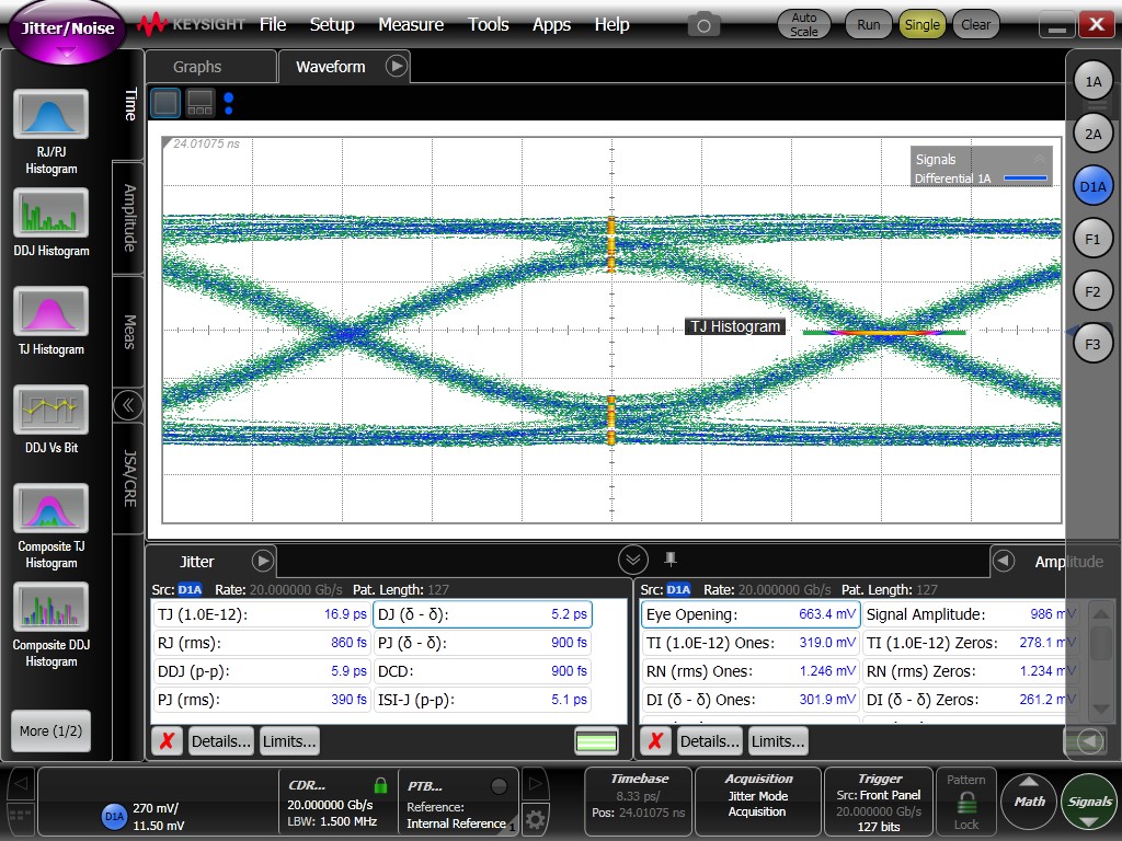 Figure 5-6 Jitter
Decomposition of 20Gbps PRBS-7 Signals in TI Evaluation Board Through a Typical
TMUXHS4412 Channels