SLOS417D October   2003  – November 2015 TPA2010D1

PRODUCTION DATA.  

  1. Features
  2. Applications
  3. Description
  4. Device Comparison Table
  5. Pin Configuration and Functions
  6. Specifications
    1. 6.1 Absolute Maximum Ratings
    2. 6.2 ESD Ratings
    3. 6.3 Recommended Operating Conditions
    4. 6.4 Thermal Information
    5. 6.5 Electrical Characteristics
    6. 6.6 Operating Characteristics
    7. 6.7 Dissipation Ratings
    8. 6.8 Typical Characteristics
  7. Parameter Measurement Information
  8. Detailed Description
    1. 8.1 Overview
    2. 8.2 Functional Block Diagram
    3. 8.3 Feature Description
      1. 8.3.1 Fully Differential Amplifier
      2. 8.3.2 Advantages of Fully Differential Amplifiers
      3. 8.3.3 Efficiency and Thermal Information
      4. 8.3.4 Eliminating the Output Filter With the TPA2010D1
        1. 8.3.4.1 Effect on Audio
        2. 8.3.4.2 Traditional Class-D Modulation Scheme
        3. 8.3.4.3 TPA2010D1 Modulation Scheme
        4. 8.3.4.4 Efficiency: Use a Filter With the Traditional Class-D Modulation Scheme
        5. 8.3.4.5 Effects of Applying a Square Wave into a Speaker
        6. 8.3.4.6 When to Use an Output Filter
    4. 8.4 Device Functional Modes
      1. 8.4.1 Summing Input Signals with the TPA2010D1
        1. 8.4.1.1 Summing Two Differential Inputs
        2. 8.4.1.2 Summing a Differential Input Signal and a Single-Ended Input Signal
        3. 8.4.1.3 TPA2010D1 Summing Two Single-Ended Inputs
      2. 8.4.2 Shutdown Mode
  9. Application and Implementation
    1. 9.1 Application Information
    2. 9.2 Typical Applications
      1. 9.2.1 TPA200110D1 With Differential Input
        1. 9.2.1.1 Design Requirements
        2. 9.2.1.2 Detailed Design Procedure
          1. 9.2.1.2.1 Input Resistors (RI)
          2. 9.2.1.2.2 Decoupling Capacitor (CS)
        3. 9.2.1.3 Application Curves
      2. 9.2.2 TPA20010D1 With Differential Input and Input Capacitors
        1. 9.2.2.1 Design Requirements
        2. 9.2.2.2 Detailed Design Procedure
          1. 9.2.2.2.1 Input Capacitors (CI)
        3. 9.2.2.3 Application Curves
      3. 9.2.3 TPA20010D1 with Single-Ended Input
        1. 9.2.3.1 Design Requirements
        2. 9.2.3.2 Detailed Design Procedure
        3. 9.2.3.3 Application Curves
  10. 10Power Supply Recommendations
    1. 10.1 Power Supply Decoupling Capacitors
  11. 11Layout
    1. 11.1 Layout Guidelines
    2. 11.2 Board Layout
      1. 11.2.1 Component Location
      2. 11.2.2 Trace Width
    3. 11.3 Layout Example
  12. 12Device and Documentation Support
    1. 12.1 Device Support
      1. 12.1.1 Third-Party Products Disclaimer
    2. 12.2 Community Resources
    3. 12.3 Trademarks
    4. 12.4 Electrostatic Discharge Caution
    5. 12.5 Glossary
  13. 13Mechanical, Packaging, and Orderable Information

Package Options

Mechanical Data (Package|Pins)
Thermal pad, mechanical data (Package|Pins)
Orderable Information

13 Mechanical, Packaging, and Orderable Information

The following pages include mechanical, packaging, and orderable information. This information is the most current data available for the designated devices. This data is subject to change without notice and revision of this document. For browser-based versions of this data sheet, refer to the left-hand navigation.
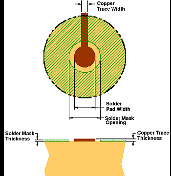
TPA2010D1 ai_land_los417.gif Figure 42. Land Pattern Dimensions

Table 3. Land Pattern Dimensions

SOLDER PAD
DEFINITIONS
COPPER PAD SOLDER MASK
OPENING
COPPER
THICKNESS
STENCIL
OPENING
STENCIL
THICKNESS
Nonsolder mask
defined (NSMD)
275 µm
(+0.0, –25 µm)
375 µm
(+0.0, –25 µm)
1 oz max (32 µm) 275 µm × 275 µm Sq.
(rounded corners)
125 µm thick