SLOS417D October   2003  – November 2015 TPA2010D1

PRODUCTION DATA.  

  1. Features
  2. Applications
  3. Description
  4. Device Comparison Table
  5. Pin Configuration and Functions
  6. Specifications
    1. 6.1 Absolute Maximum Ratings
    2. 6.2 ESD Ratings
    3. 6.3 Recommended Operating Conditions
    4. 6.4 Thermal Information
    5. 6.5 Electrical Characteristics
    6. 6.6 Operating Characteristics
    7. 6.7 Dissipation Ratings
    8. 6.8 Typical Characteristics
  7. Parameter Measurement Information
  8. Detailed Description
    1. 8.1 Overview
    2. 8.2 Functional Block Diagram
    3. 8.3 Feature Description
      1. 8.3.1 Fully Differential Amplifier
      2. 8.3.2 Advantages of Fully Differential Amplifiers
      3. 8.3.3 Efficiency and Thermal Information
      4. 8.3.4 Eliminating the Output Filter With the TPA2010D1
        1. 8.3.4.1 Effect on Audio
        2. 8.3.4.2 Traditional Class-D Modulation Scheme
        3. 8.3.4.3 TPA2010D1 Modulation Scheme
        4. 8.3.4.4 Efficiency: Use a Filter With the Traditional Class-D Modulation Scheme
        5. 8.3.4.5 Effects of Applying a Square Wave into a Speaker
        6. 8.3.4.6 When to Use an Output Filter
    4. 8.4 Device Functional Modes
      1. 8.4.1 Summing Input Signals with the TPA2010D1
        1. 8.4.1.1 Summing Two Differential Inputs
        2. 8.4.1.2 Summing a Differential Input Signal and a Single-Ended Input Signal
        3. 8.4.1.3 TPA2010D1 Summing Two Single-Ended Inputs
      2. 8.4.2 Shutdown Mode
  9. Application and Implementation
    1. 9.1 Application Information
    2. 9.2 Typical Applications
      1. 9.2.1 TPA200110D1 With Differential Input
        1. 9.2.1.1 Design Requirements
        2. 9.2.1.2 Detailed Design Procedure
          1. 9.2.1.2.1 Input Resistors (RI)
          2. 9.2.1.2.2 Decoupling Capacitor (CS)
        3. 9.2.1.3 Application Curves
      2. 9.2.2 TPA20010D1 With Differential Input and Input Capacitors
        1. 9.2.2.1 Design Requirements
        2. 9.2.2.2 Detailed Design Procedure
          1. 9.2.2.2.1 Input Capacitors (CI)
        3. 9.2.2.3 Application Curves
      3. 9.2.3 TPA20010D1 with Single-Ended Input
        1. 9.2.3.1 Design Requirements
        2. 9.2.3.2 Detailed Design Procedure
        3. 9.2.3.3 Application Curves
  10. 10Power Supply Recommendations
    1. 10.1 Power Supply Decoupling Capacitors
  11. 11Layout
    1. 11.1 Layout Guidelines
    2. 11.2 Board Layout
      1. 11.2.1 Component Location
      2. 11.2.2 Trace Width
    3. 11.3 Layout Example
  12. 12Device and Documentation Support
    1. 12.1 Device Support
      1. 12.1.1 Third-Party Products Disclaimer
    2. 12.2 Community Resources
    3. 12.3 Trademarks
    4. 12.4 Electrostatic Discharge Caution
    5. 12.5 Glossary
  13. 13Mechanical, Packaging, and Orderable Information

Package Options

Mechanical Data (Package|Pins)
Thermal pad, mechanical data (Package|Pins)
Orderable Information

5 Pin Configuration and Functions

YZF and YEF Package
9-Pin DSBGA
Top View
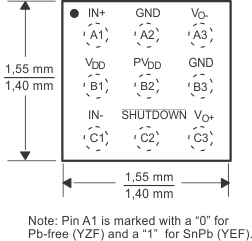
TPA2010D1 package_los417.gif

Pin Functions

PIN I/O DESCRIPTION
NO. NAME
A1 IN+ I Positive differential input
A2 GND I High-current ground
A3 VO- O Negative BTL output
B1 VDD I Power supply
B2 PVDD I Power supply
B3 GND I High-current ground
C1 IN- I Negative differential input
C2 SHUTDOWN I Shutdown terminal (active low logic)
C3 VO+ O Positive BTL output