SLOS520A August 2007 – March 2016 TPA2013D1
PRODUCTION DATA.
- 1 Features
- 2 Applications
- 3 Description
- 4 Revision History
- 5 Device Comparison Table
- 6 Pin Configuration and Functions
-
7 Specifications
- 7.1 Absolute Maximum Ratings
- 7.2 ESD Ratings
- 7.3 Recommended Operating Conditions
- 7.4 Thermal Information
- 7.5 DC Characteristics
- 7.6 Boost Converter DC Characteristics
- 7.7 Class D Amplifier DC Characteristics
- 7.8 AC Characteristics
- 7.9 Class D Amplifier AC Characteristics
- 7.10 Dissipation Ratings
- 7.11 Typical Characteristics
- 8 Parameter Measurement Information
- 9 Detailed Description
-
10Application and Implementation
- 10.1 Application Information
- 10.2
Typical Applications
- 10.2.1
TPA2013D1 With Differential Input Signal
- 10.2.1.1 Design Requirements
- 10.2.1.2 Detailed Design Procedure
- 10.2.1.3 Application Curves
- 10.2.2 Bypassing the Boost Converter
- 10.2.3 Stereo Operation Application
- 10.2.4 LED Driver for Digital Still Cameras
- 10.2.5 Design Requirements
- 10.2.6 Detailed Design Procedure
- 10.2.7 Application Curves
- 10.2.1
TPA2013D1 With Differential Input Signal
- 11Power Supply Recommendations
- 12Layout
- 13Device and Documentation Support
- 14Mechanical, Packaging, and Orderable Information
Package Options
Mechanical Data (Package|Pins)
Thermal pad, mechanical data (Package|Pins)
- RGP|20
Orderable Information
10 Application and Implementation
NOTE
Information in the following applications sections is not part of the TI component specification, and TI does not warrant its accuracy or completeness. TI’s customers are responsible for determining suitability of components for their purposes. Customers should validate and test their design implementation to confirm system functionality.
10.1 Application Information
These typical connection diagrams highlight the required external components and system level connections for proper operation of the device. Each of these configurations can be realized using the Evaluation Modules (EVMs) for the device. These flexible modules allow full evaluation of the device in the most common modes of operation. Any design variation can be supported by TI through schematic and layout reviews. Visit e2e.ti.com for design assistance, and join the audio amplifier discussion forum for additional information.
10.2 Typical Applications
10.2.1 TPA2013D1 With Differential Input Signal
 Figure 33. Typical Application Schematic With Differential Input Signals
10.2.1.1 Design Requirements
For this design example, use the parameters listed in Table 5.
Table 5. Design Parameters
| DESIGN PARAMETERS | EXAMPLE VALUE |
|---|---|
| Power Supply | 3.6 V |
| Enable Inputs | High > 1.3 V |
| Low < 0.6 V | |
| Speaker | 8 Ω |
10.2.1.2 Detailed Design Procedure
10.2.1.2.1 Setting the Boost Voltage
Use Equation 1 to determine the value of R1 for a given VCC. The maximum recommended value for VCC is
5.5 V. The typical value of the VCCFB pin is 500 mV. The current through the resistor divider should be about 100 times greater than the current into the VCCFB pin, typically 0.01 μA. Based on those two values, the recommended value of R2 is 500 kΩ. VCC must be greater than 3 V and less than or equal to 5.5 V.

10.2.1.2.2 Inductor Selection
10.2.1.2.2.1 Surface Mount Inductors
Working inductance decreases as inductor current increases. If the drop in working inductance is severe enough, it may cause the boost converter to become unstable, or cause the TPA2013D1 to reach its current limit at a lower output power than expected. Inductor vendors specify currents at which inductor values decrease by a specific percentage. This can vary by 10% to 35%. Inductance is also affected by DC current and temperature.
10.2.1.2.2.2 TPA2013D1 Inductor Equations
Inductor current rating is determined by the requirements of the load. The inductance is determined by two factors: the minimum value required for stability and the maximum ripple current permitted in the application.
Use Equation 2 to determine the required current rating. Equation 2 shows the approximate relationship between the average inductor current, IL, to the load current, load voltage, and input voltage (ICC, VCC, and VDD, respectively). Insert ICC, VCC, and VDD into Equation 2 to solve for IL. The inductor must maintain at least 90% of its initial inductance value at this current.

The minimum working inductance is 2.2 μH. A lower value may cause instability.
Ripple current, ΔIL, is peak-to-peak variation in inductor current. Smaller ripple current reduces core losses in the inductor as well as the potential for EMI. Use Equation 3 to determine the value of the inductor, L. Equation 3 shows the relationship between inductance L, VDD, VCC, the switching frequency, fboost, and ΔIL. Insert the maximum acceptable ripple current into Equation 3 to solve for L.

ΔIL is inversely proportional to L. Minimize ΔIL as much as is necessary for a specific application. Increase the inductance to reduce the ripple current.
NOTE
Making the inductance too large prevents the boost converter from responding to fast load changes properly. Typical inductor values for the TPA2013D1 are 4.7 μH to 6.8 μH.
Select an inductor with a small DC resistance, DCR. DCR reduces the output power due to the voltage drop across the inductor.
10.2.1.2.3 Capacitor Selection
10.2.1.2.3.1 Surface Mount Capacitors
Temperature and applied DC voltage influence the actual capacitance of high-K materials.
Table 6 shows the relationship between the different types of high-K materials and their associated tolerances, temperature coefficients, and temperature ranges. Notice that a capacitor made with X5R material can lose up to 15% of its capacitance within its working temperature range.
High-K material is very sensitive to applied DC voltage. X5R capacitors can have losses ranging from 15 to 45% of their initial capacitance with only half of their DC-rated voltage applied. For example, if 5 Vdc is applied to a 10-V, 1-μF X5R capacitor, the measured capacitance at that point may show 0.85 μF, 0.55 μF, or somewhere in between. Y5V capacitors have losses that can reach or exceed 50% to 75% of their rated value.
In an application, the working capacitance of components made with high-K materials is generally much lower than nominal capacitance. A worst-case result with a typical X5R material might be –10% tolerance, –15% temperature effect, and –45% DC-voltage effect at 50% of the rated voltage. This particular case would result in a working capacitance of 42% (0.9 × 0.85 × 0.55) of the nominal value.
Select high-K ceramic capacitors according to the following rules:
- Use capacitors made of materials with temperature coefficients of X5R, X7R, or better.
- Use capacitors with DC-voltage ratings of at least twice the application voltage. Use minimum 10-V capacitors for the TPA2013D1.
- Choose a capacitance value at least twice the nominal value calculated for the application. Multiply the nominal value by a factor of 2 for safety. If a 10-μF capacitor is required, use 20 μF.
The preceding rules and recommendations apply to capacitors used in connection with the TPA2013D1. The TPA2013D1 cannot meet its performance specifications if the rules and recommendations are not followed.
Table 6. Typical Tolerance and Temperature Coefficient of Capacitance by Material
| MATERIAL | COG/NPO | X7R | X5R |
|---|---|---|---|
| Typical Tolerance | ±5% | ±10% | 80/–20% |
| Temperature Coefficient | ±30ppm | ±15% | 22/–82% |
| Temperature Range, °C | –55/125°C | –55/125°C | –30/85°C |
10.2.1.2.3.2 TPA2013D1 Capacitor Equations
The value of the boost capacitor is determined by the minimum value of working capacitance required for stability and the maximum voltage ripple allowed on VCC in the application. The minimum value of working capacitance is 10 μF. Do not use any component with a working capacitance less than 10 μF.
For X5R or X7R ceramic capacitors, Equation 4 shows the relationship between the boost capacitance, C, to load current, load voltage, ripple voltage, input voltage, and switching frequency (ICC, VCC, ΔV, VDD, fboost respectively). Insert the maximum allowed ripple voltage into Equation 4 to solve for C. A factor of 2 is included to implement the rules and specifications listed earlier.

For aluminum or tantalum capacitors, Equation 5 shows the relationship between the boost capacitance, C, to load current, load voltage, ripple voltage, input voltage, and switching frequency (ICC, VCC, ΔV, VDD, fboost respectively). Insert the maximum allowed ripple voltage into Equation 5 to solve for C. Solve this equation assuming ESR is zero.

Capacitance of aluminum and tantalum capacitors is normally not sensitive to applied voltage, so there is no factor of 2 included in Equation 5. However, the ESR in aluminum and tantalum capacitors can be significant. Choose an aluminum or tantalum capacitor with ESR around 30 mΩ. For best perfornamce using of tantalum capacitor, use at least a 10-V rating.
NOTE
Tantalum capacitors must generally be used at voltages of half their ratings or less.
10.2.1.2.4 Recommended Inductor and Capacitor Values by Application
Use Table 7 as a guide for determining the proper inductor and capacitor values.
Table 7. Recommended Values
| CLASS-D OUTPUT POWER (W)(1) |
CLASS-D LOAD (Ω) |
MINIMUM VDD
(V) |
REQUIRED VCC (V) |
MAX IL
(A) |
L (μH) |
INDUCTOR VENDOR PART NUMBERS |
MAX ΔV (mVpp) |
C(2)
(μF) |
CAPACITOR VENDOR PART NUMBERS |
|---|---|---|---|---|---|---|---|---|---|
| 1 | 8 | 3 | 4.3 | 0.70 | 3.3 | 30 | 10 | ||
| Toko DE2812C Coilcraft DO3314 Murata LQH3NPN3R3NG0 |
Kemet C1206C106K8PACTU Murata GRM32ER61A106KA01B Taiyo Yuden LMK316BJ106ML-T |
||||||||
| 1.6 | 8 | 3 | 5.5 | 1.13 | 4.7 | 30 | 22 | ||
| Murata LQH32PN4R7NN0 Toko DE4514C Coilcraft LPS4018-472 |
Murata GRM32ER71A226KE20L Taiyo Yuden LMK316BJ226ML-T |
||||||||
| 2 | 4 | 3 | 4.6 | 1.53 | 3.3 | 30 | 33 | ||
| Murata LQH55PN3R3NR0 Toko DE4514C |
TDK C4532X5R1A336M | ||||||||
| 2.3 | 4 | 1.8 | 5.5 | 2 | 6.2 | 30 | 47 | ||
| Sumida CDRH5D28NP-6R2NC |
Murata GRM32ER61A476KE20L Taiyo Yuden LMK325BJ476MM-T |
||||||||
10.2.1.2.5 Components Location and Selection
10.2.1.2.5.1 Decoupling Capacitors
The TPA2013D1 is a high-performance Class-D audio amplifier that requires adequate power-supply decoupling to ensure the efficiency is high and total harmonic distortion (THD) is low. Place a low equivalent-series-resistance (ESR) ceramic capacitor, typically 1 μF, as close as possible to the device VDD lead. This choice of capacitor and placement helps with higher frequency transients, spikes, or digital hash on the line. Additionally, placing this decoupling capacitor close to the TPA2013D1 is important for the efficiency of the Class-D amplifier, because any resistance or inductance in the trace between the device and the capacitor can cause a loss in efficiency. Place a capacitor of 10 μF or greater between the power supply and the boost inductor. The capacitor filters out high-frequency noise. More importantly, it acts as a charge reservoir, providing energy more quickly than the board supply, thus helping to prevent any droop.
10.2.1.2.5.2 Input Capacitors
The TPA2013D1 does not require input coupling capacitors if the design uses a differential source that is biased within the common mode input range. Use input coupling capacitors if the input signal is not biased within the recommended common-mode input range, if high-pass filtering is needed, or if using a single-ended source.
The input capacitors and input resistors form a high-pass filter with the corner frequency, fc, determined in Equation 6.

The value of the input capacitor is important to consider as it directly affects the bass (low frequency) performance of the circuit. Speakers in wireless phones cannot usually respond well to low frequencies, so the corner frequency can be set to block low frequencies in this application. Not using input capacitors can increase output offset.
Use Equation 7 to find the required the input coupling capacitance.

Any mismatch in capacitance between the two inputs causes a mismatch in the corner frequencies. Choose capacitors with a tolerance of ±10% or better.
10.2.2 Bypassing the Boost Converter
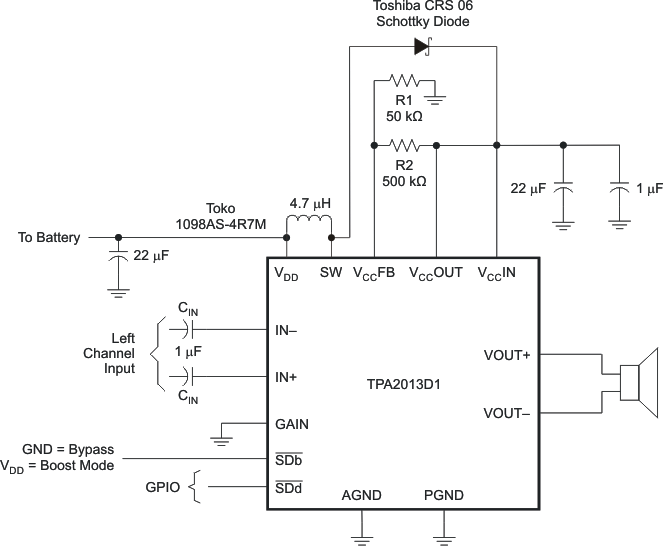
Bypass the boost converter to drive the Class-D amplifier directly from the battery. Place a Shottky diode between the SW pin and the VCCIN pin. Select a diode that has an average forward current rating of at least 1 A, reverse breakdown voltage of 10 V or greater, and a forward voltage as small as possible. See Figure 34 for an example of a circuit designed to bypass the boost converter.
Do not configure the circuit to bypass the boost converter if VDD is higher than VCC when the boost converter is enabled (SDb ≥ 1.3 V); VDD must be lower than VCC for proper operation. VDD may be set to any voltage within the recommended operating range when the boost converter is disabled (SDb ≤ 0.3 V).
Place a logic high on SDb to place the TPA2013D1 in boost mode. Place a logic low on SDb to place the TPA2013D1 in bypass mode.
 Figure 34. Bypass Circuit
10.2.2.1 Design Requirements
For this design example, use the parameters listed in Table 5.
10.2.2.2 Detailed Design Procedure
For the design procedure, see Detailed Design Procedure.
10.2.2.3 Application Curves
For application curves, see the figures listed in Table 8.
10.2.3 Stereo Operation Application
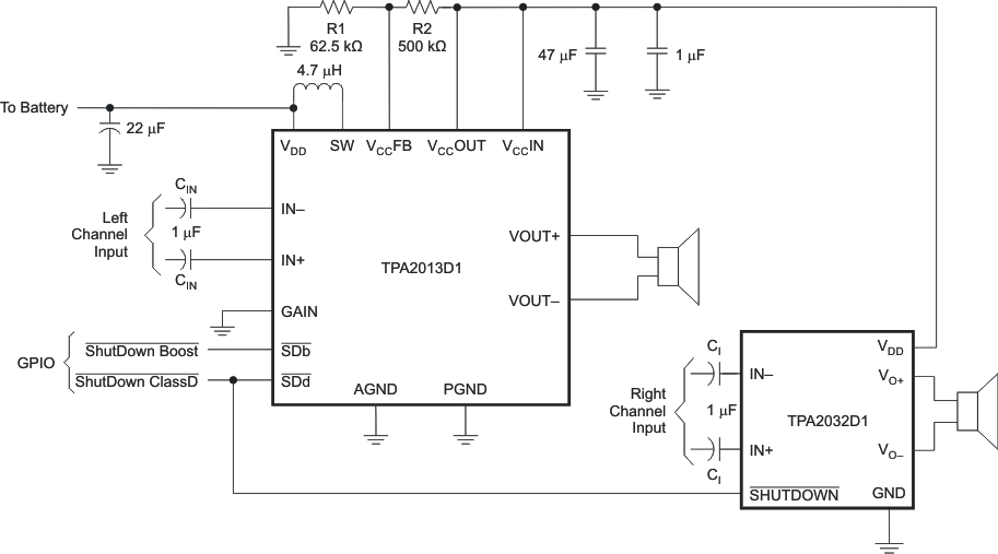
Use the boost converter of the TPA2013D1 to supply the power for another audio amplifier when stereo operation is required. Ensure the gains of the amplifiers match each other. This prevents one channel from sounding louder than the other. Use Equation 1 through Equation 5 to determine R1, R2, boost inductor, and the boost capacitor values. Figure 35 is an example schematic. The TPA2032D1 is a good choice for this application; the gain is internally set to 2 V/V, the power supply is compatible with VCCOUT of the TPA2013D1, and the output power of the TPA2032D1 is on par with the TPA2013D1.
 Figure 35. TPA2013D1 in Stereo With the TPA2032D1
10.2.3.1 Design Requirements
For this design example, use the parameters listed in Table 5.
10.2.3.2 Detailed Design Procedure
For the design procedure, see Detailed Design Procedure.
10.2.3.3 Application Curves
For application curves, see the figures listed in Table 8.
10.2.4 LED Driver for Digital Still Cameras
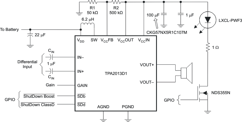
Use the boost converter of the TPA2013D1 as a power supply for the flash LED of a digital still camera. Use a microprocessor or other device or synchronize the flash to shutter sound that typically comes from the speaker of a digital still camera. Figure 36 shows a typical circuit for this application. LEDs, switches, and other components varies by application.
 Figure 36. LED Driver
10.2.5 Design Requirements
For this design example, use the parameters listed in Table 5.
10.2.6 Detailed Design Procedure
For the design procedure, see Detailed Design Procedure.
10.2.7 Application Curves
For application curves, see the figures listed in Table 8.