SLOS660C January 2010 – October 2015 TPA2028D1
PRODUCTION DATA.
- 1 Features
- 2 Applications
- 3 Description
- 4 Revision History
- 5 Device Comparison Table
- 6 Pin Configuration and Functions
- 7 Specifications
- 8 Parameter Measurement Information
- 9 Detailed Description
- 10Application and Implementation
- 11Power Supply Recommendations
- 12Layout
- 13Device and Documentation Support
- 14Mechanical, Packaging, and Orderable Information
Package Options
Mechanical Data (Package|Pins)
- YZF|9
Thermal pad, mechanical data (Package|Pins)
Orderable Information
10 Application and Implementation
NOTE
Information in the following applications sections is not part of the TI component specification, and TI does not warrant its accuracy or completeness. TI’s customers are responsible for determining suitability of components for their purposes. Customers should validate and test their design implementation to confirm system functionality.
10.1 Application Information
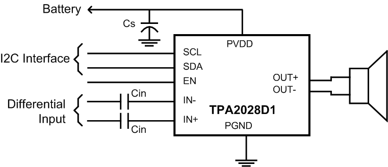
These typical connection diagrams highlight the required external components and system level connections for proper operation of the device. Each of these configurations can be realized using the Evaluation Modules (EVMs) for the device. These flexible modules allow full evaluation of the device in the most common modes of operation. Any design variation can be supported by TI through schematic and layout reviews. Visit e2e.ti.com for design assistance and join the audio amplifier discussion forum for additional information.
10.2 Typical Application
 Figure 49. TPA2028D1 Application Schematic
10.2.1 Design Requirements
For this design example, use the parameters listed in Table 13.
Table 13. Design Parameters
| DESIGN PARAMETER | EXAMPLE VALUE |
|---|---|
| Power supply | 5 V |
| Supply current | 2-A Maximum |
| Audio input voltage | 0.5 V to VDD - 0.5 V |
| Speaker impedance | 8 Ω |
10.2.2 Detailed Design Procedure
10.2.2.1 Decoupling Capacitor CS
The TPA2028D1 is a high-performance Class-D audio amplifier that requires adequate power supply decoupling to ensure the efficiency is high and total harmonic distortion (THD) is low. For higher frequency transients, spikes, or digital hash on the line, a good low equivalent-series-resistance (ESR) 1-μF ceramic capacitor (typically) placed as close as possible to the device PVDD lead works best. Placing this decoupling capacitor close to the TPA2028D1 is important for the efficiency of the Class-D amplifier, because any resistance or inductance in the trace between the device and the capacitor can cause a loss in efficiency. For filtering lower-frequency noise signals, a 4.7 μF or greater capacitor placed near the audio power amplifier would also help, but it is not required in most applications because of the high PSRR of this device.
10.2.2.2 Input Capacitors CI)
TPA2028D1 requires input capacitors to ensure low output offset and low pop.
The input capacitors and input resistors form a high-pass filter with the corner frequency, fC, determined in Equation 5.

The value of the input capacitor is important to consider as it directly affects the bass (low frequency) performance of the circuit. Speakers in wireless phones cannot usually respond well to low frequencies, so the corner frequency can be set to block low frequencies in this application. Not using input capacitors can increase output offset. Equation 6 is used to solve for the input coupling capacitance. If the corner frequency is within the audio band, the capacitors should have a tolerance of ±10% or better, because any mismatch in capacitance causes an impedance mismatch at the corner frequency and below.
