SLOS708G April 2012 – December 2017 TPA3116D2 , TPA3118D2 , TPA3130D2
PRODUCTION DATA.
- 1 Features
- 2 Applications
- 3 Description
- 4 Revision History
- 5 Pin Configuration and Functions
- 6 Specifications
-
7 Detailed Description
- 7.1 Overview
- 7.2 Functional Block Diagram
- 7.3
Feature Description
- 7.3.1 Gain Setting and Master and Slave
- 7.3.2 Input Impedance
- 7.3.3 Startup and Shutdown Operation
- 7.3.4 PLIMIT Operation
- 7.3.5 GVDD Supply
- 7.3.6 BSPx AND BSNx Capacitors
- 7.3.7 Differential Inputs
- 7.3.8 Device Protection System
- 7.3.9 DC Detect Protection
- 7.3.10 Short-Circuit Protection and Automatic Recovery Feature
- 7.3.11 Thermal Protection
- 7.3.12 Device Modulation Scheme
- 7.3.13 Efficiency: LC Filter Required with the Traditional Class-D Modulation Scheme
- 7.3.14 Ferrite Bead Filter Considerations
- 7.3.15 When to Use an Output Filter for EMI Suppression
- 7.3.16 AM Avoidance EMI Reduction
- 7.4 Device Functional Modes
- 8 Application and Implementation
- 9 Power Supply Recommendations
- 10Layout
- 11Device and Documentation Support
- 12Mechanical, Packaging, and Orderable Information
Package Options
Mechanical Data (Package|Pins)
- DAP|32
Thermal pad, mechanical data (Package|Pins)
- DAP|32
Orderable Information
6 Specifications
6.1 Absolute Maximum Ratings
over operating free-air temperature range (unless otherwise noted)(1)| MIN | MAX | UNIT | ||
|---|---|---|---|---|
| Supply voltage, VCC | PVCC, AVCC | –0.3 | 30 | V |
| Input voltage, VI | INPL, INNL, INPR, INNR | –0.3 | 6.3 | V |
| PLIMIT, GAIN / SLV, SYNC | –0.3 | GVDD+0.3 | V | |
| AM0, AM1, AM2, MUTE, SDZ, MODSEL | –0.3 | PVCC+0.3 | V | |
| Slew rate, maximum(2) | AM0, AM1, AM2, MUTE, SDZ, MODSEL | 10 | V/ms | |
| Operating free-air temperature, TA | –40 | 85 | °C | |
| Operating junction temperature , TJ | –40 | 150 | °C | |
| Storage temperature, Tstg | –40 | 125 | °C | |
(1) Stresses beyond those listed under absolute maximum ratings may cause permanent damage to the device. These are stress ratings only, and functional operation of the device at these or any other conditions beyond those indicated under recommended operating conditions is not implied. Exposure to absolute-maximum-rated conditions for extended periods may affect device reliability.
(2) 100 kΩ series resistor is needed if maximum slew rate is exceeded.
6.2 ESD Ratings
| VALUE | UNIT | |||
|---|---|---|---|---|
| V(ESD) | Electrostatic discharge | Human-body model (HBM), per ANSI/ESDA/JEDEC JS-001(1) | ±2000 | V |
| Charged-device model (CDM), per JEDEC specification JESD22-C101(2) | ±500 | |||
(1) JEDEC document JEP155 states that 500-V HBM allows safe manufacturing with a standard ESD control process.
(2) JEDEC document JEP157 states that 250-V CDM allows safe manufacturing with a standard ESD control process. .
6.3 Recommended Operating Conditions
over operating free-air temperature range (unless otherwise noted)| MIN | NOM | MAX | UNIT | ||||
|---|---|---|---|---|---|---|---|
| VCC | Supply voltage | PVCC, AVCC | 4.5 | 26 | V | ||
| VIH | High-level input voltage | AM0, AM1, AM2, MUTE, SDZ, SYNC, MODSEL | 2 | V | |||
| VIL | Low-level input voltage | AM0, AM1, AM2, MUTE, SDZ, SYNC, MODSEL | 0.8 | V | |||
| VOL | Low-level output voltage | FAULTZ, RPULL-UP = 100 kΩ, PVCC = 26 V | 0.8 | V | |||
| IIH | High-level input current | AM0, AM1, AM2, MUTE, SDZ, MODSEL (VI = 2 V, VCC = 18 V) | 50 | µA | |||
| RL(BTL) | Minimum load Impedance | Output filter: L = 10 µH, C = 680 nF | TPA3116D2, TPA3118D2 | 3.2 | 4 | Ω | |
| TPA3130D2 | 5.6 | 8 | |||||
| RL(PBTL) | Output filter: L = 10 µH, C = 1 µF | TPA3116D2, TPA3118D2 | 1.6 | ||||
| TPA3130D2 | 3.2 | 4 | |||||
| Lo | Output-filter Inductance | Minimum output filter inductance under short-circuit condition | 1 | µH | |||
6.4 Thermal Information
| THERMAL METRIC(1) | TPA3130D2 | TPA3118D2 | TPA3116D2 | UNIT | |
|---|---|---|---|---|---|
| DAP(2) | DAP(3) | DAD(4) | |||
| 32 PINS | 32 PINS | 32 PINS | |||
| RθJA | Junction-to-ambient thermal resistance | 36 | 22 | 14 | °C/W |
| ψJT | Junction-to-top characterization parameter | 0.4 | 0.3 | 1.2 | |
| ψJB | Junction-to-board characterization parameter | 5.9 | 4.7 | 5.7 | |
(1) For more information about traditional and new thermal metrics, see the Semiconductor and IC Package Thermal Metrics application report.
(2) For the PCB layout please see the TPA3130D2EVM user guide.
(3) For the PCB layout please see the TPA3118D2EVM user guide.
(4) The heat sink drawing used for the thermal model data are shown in the application section, size: 14mm wide, 50mm long, 25mm high.
6.5 DC Electrical Characteristics
TA = 25°C, AVCC = PVCC = 12 V to 24 V, RL = 4 Ω (unless otherwise noted)6.6 AC Electrical Characteristics
TA = 25°C, AVCC = PVCC = 12 V to 24 V, RL = 4 Ω (unless otherwise noted)| PARAMETER | TEST CONDITIONS | MIN | TYP | MAX | UNIT | |
|---|---|---|---|---|---|---|
| KSVR | Power supply ripple rejection | 200 mVPP ripple at 1 kHz, Gain = 20 dB, Inputs AC-coupled to GND | –70 | dB | ||
| PO | Continuous output power | THD+N = 10%, f = 1 kHz, PVCC = 14.4 V | 25 | W | ||
| THD+N = 10%, f = 1 kHz, PVCC = 21 V | 50 | |||||
| THD+N | Total harmonic distortion + noise | VCC = 21 V, f = 1 kHz, PO = 25 W (half-power) | 0.1% | |||
| Vn | Output integrated noise | 20 Hz to 22 kHz, A-weighted filter, Gain = 20 dB | 65 | µV | ||
| –80 | dBV | |||||
| Crosstalk | VO = 1 Vrms, Gain = 20 dB, f = 1 kHz | –100 | dB | |||
| SNR | Signal-to-noise ratio | Maximum output at THD+N < 1%, f = 1 kHz, Gain = 20 dB, A-weighted | 102 | dB | ||
| fOSC | Oscillator frequency | AM2=0, AM1=0, AM0=0 | 376 | 400 | 424 | kHz |
| AM2=0, AM1=0, AM0=1 | 470 | 500 | 530 | |||
| AM2=0, AM1=1, AM0=0 | 564 | 600 | 636 | |||
| AM2=0, AM1=1, AM0=1 | 940 | 1000 | 1060 | |||
| AM2=1, AM1=0, AM0=0 | 1128 | 1200 | 1278 | |||
| AM2=1, AM1=0, AM0=1 | Reserved | |||||
| AM2=1, AM1=1, AM0=0 | ||||||
| AM2=1, AM1=1, AM0=1 | ||||||
| Thermal trip point | 150+ | °C | ||||
| Thermal hysteresis | 15 | °C | ||||
| Over current trip point | TPA3130D2 | 4.5 | A | |||
| TPA3118D2, TPA3116D2 | 7.5 | |||||
6.7 Typical Characteristics
fs = 400 kHz, BD Mode (unless otherwise noted)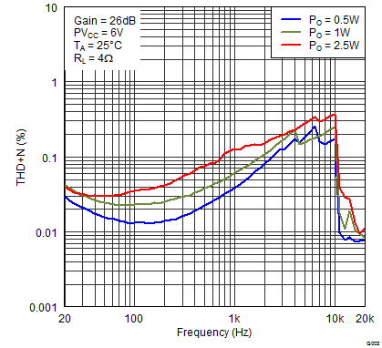 Figure 1. Total Harmonic Distortion + Noise (BTL) vs Frequency
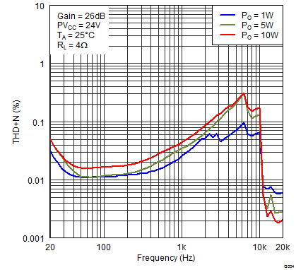 Figure 3. Total Harmonic Distortion + Noise (BTL) vs Frequency
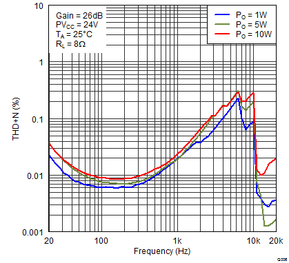 Figure 5. Total Harmonic Distortion + Noise (BTL) vs Frequency
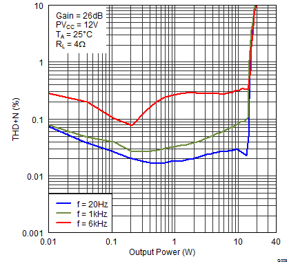 Figure 7. Total Harmonic Distortion + Noise (BTL) vs Output Power
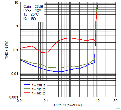 Figure 9. Total Harmonic Distortion + Noise (BTL) vs Output Power
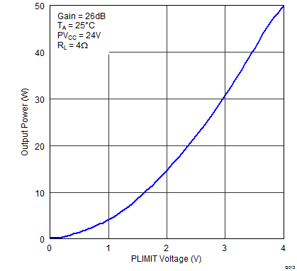 Figure 11. Output Power (BTL) vs Plimit Voltage
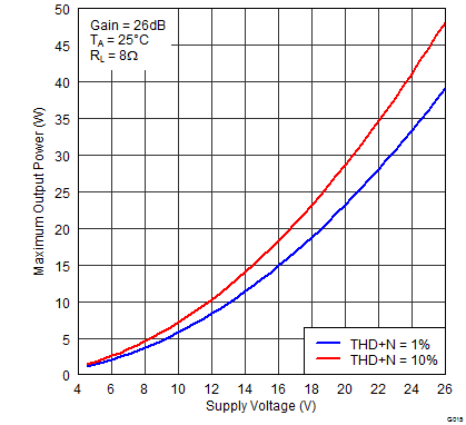 Figure 13. Maximum Output Power (BTL) vs Supply Voltage
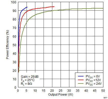 Figure 15. Power Efficiency (BTL) vs Output Power
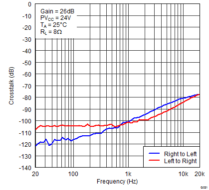 Figure 17. Crosstalk vs Frequency
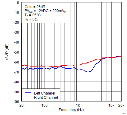 Figure 19. Supply Ripple Rejection Ratio (BTL) vs Frequency
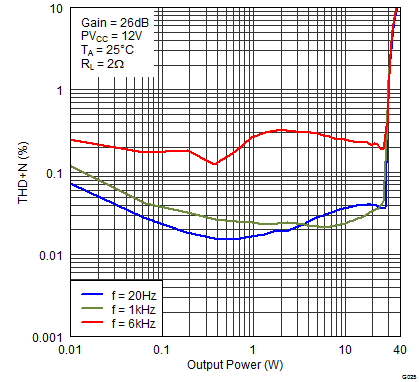 Figure 21. Total Harmonic Distortion + Noise (PBTL) vs Output Power
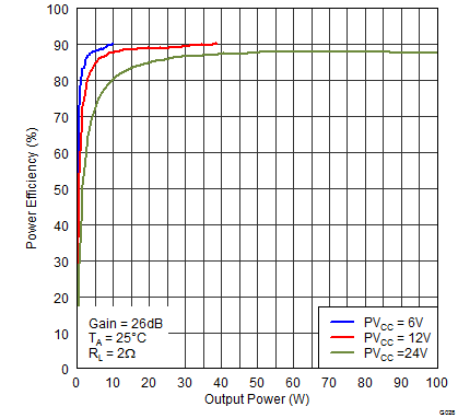 Figure 23. Power Efficiency (PBTL) vs Output Power
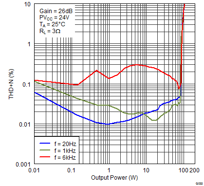 Figure 25. Total Harmonic Distortion + Noise (PBTL) vs Output Power
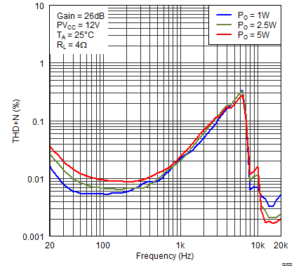 Figure 2. Total Harmonic Distortion + Noise (BTL) vs Frequency
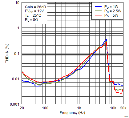 Figure 4. Total Harmonic Distortion + Noise (BTL) vs Frequency
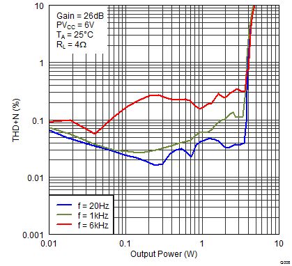 Figure 6. Total Harmonic Distortion + Noise (BTL) vs Output Power
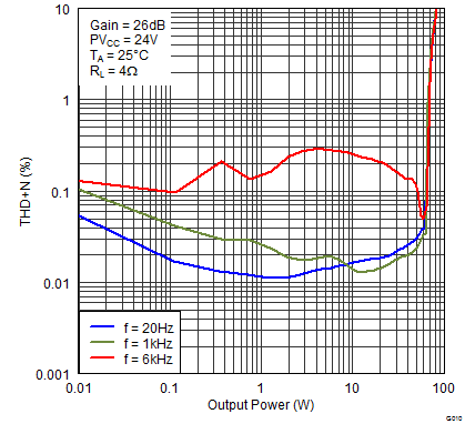 Figure 8. Total Harmonic Distortion + Noise (BTL) vs Output Power
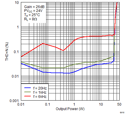 Figure 10. Total Harmonic Distortion + Noise (BTL) vs Output Power
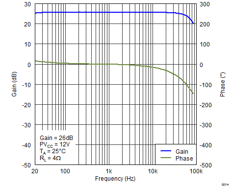 Figure 12. Gain/Phase (BTL) vs Frequency
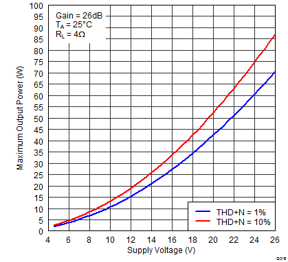 Figure 14. Maximum Output Power (BTL) vs Supply Voltage
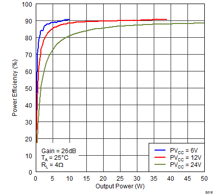 Figure 16. Power Efficiency (BTL) vs Output Power
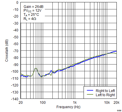 Figure 18. Crosstalk vs Frequency
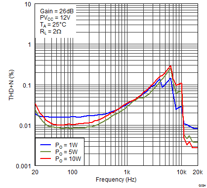 Figure 20. Total Harmonic Distortion + Noise (PBTL) vs Frequency
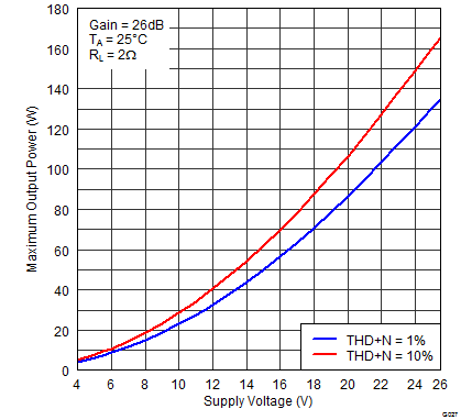 Figure 22. Maximum Output Power (PBTL) vs Supply Voltage
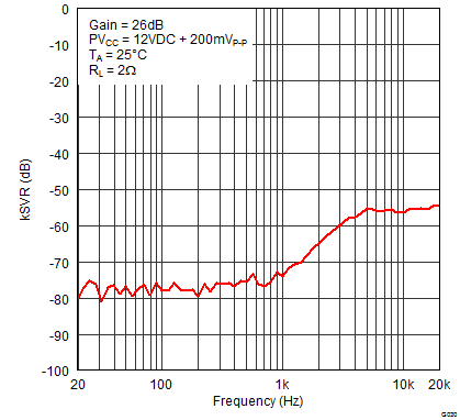 Figure 24. Supply Ripple Rejection Ratio (PBTL) vs Frequency
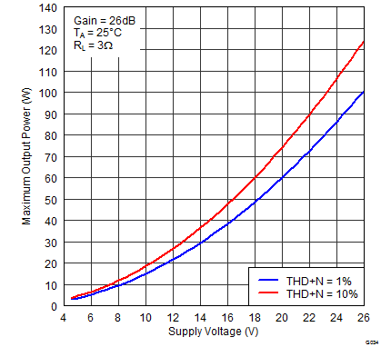 Figure 26. Maximum Output Power (PBTL) vs Supply Voltage