SLOS941C May 2016 – January 2018 TPA3128D2 , TPA3129D2
PRODUCTION DATA.
- 1 Features
- 2 Applications
- 3 Description
- 4 Revision History
- 5 Pin Configuration and Functions
- 6 Specifications
-
7 Detailed Description
- 7.1 Overview
- 7.2 Functional Block Diagram
- 7.3
Feature Description
- 7.3.1 Gain Setting and Master and Slave
- 7.3.2 Input Impedance
- 7.3.3 Startup and Shutdown Operation
- 7.3.4 PLIMIT Operation
- 7.3.5 GVDD Supply
- 7.3.6 BSPx AND BSNx Capacitors
- 7.3.7 Differential Inputs
- 7.3.8 Device Protection System
- 7.3.9 DC Detect Protection
- 7.3.10 Short-Circuit Protection and Automatic Recovery Feature
- 7.3.11 Thermal Protection
- 7.3.12 Device Modulation Scheme
- 7.3.13 Efficiency: LC Filter Required with the Traditional Class-D Modulation Scheme
- 7.3.14 Ferrite Bead Filter Considerations
- 7.3.15 When to Use an Output Filter for EMI Suppression
- 7.3.16 AM Avoidance EMI Reduction
- 7.4 Device Functional Modes
- 8 Applications and Implementation
- 9 Power Supply Recommendations
- 10Layout
- 11Device and Documentation Support
- 12Mechanical, Packaging, and Orderable Information
Package Options
Mechanical Data (Package|Pins)
- DAP|32
Thermal pad, mechanical data (Package|Pins)
- DAP|32
Orderable Information
7.3.10 Short-Circuit Protection and Automatic Recovery Feature
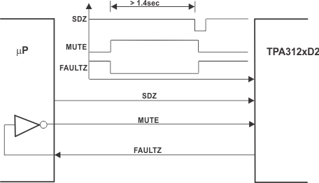
The TPA31xxD2 has protection from over current conditions caused by a short circuit on the output stage. The short circuit protection fault is reported on the FAULTZ pin as a low state. The amplifier outputs are switched to a high impedance state when the short circuit protection latch is engaged. The latch can be cleared by cycling the SDZ pin through the low state.
If automatic recovery from the short circuit protection latch is desired, connect the FAULTZ pin directly to the SDZ pin. Connecting the FAULTZ and SDZ pins allows the FAULTZ pin function to automatically drive the SDZ pin low which clears the short-circuit protection latch.
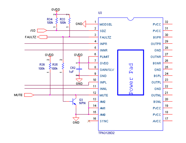
In systems where a possibility of a permanent short from the output to PVDD or to a high voltage battery like a car battery can occur, pull the MUTE pin low with the FAULTZ signal with a inverting transistor to ensure a high-Z restart, like shown in the Figure 28 below:
 Figure 28. MUTE Driven by Inverted FAULTZ
 Figure 29. Timing Requirement for SDZ