SLOS938F May 2016 – January 2020 TPA3136AD2 , TPA3136D2
PRODUCTION DATA.
- 1 Features
- 2 Applications
- 3 Description
- 4 Revision History
- 5 Device Comparison Table
- 6 Pin Configuration and Functions
- 7 Specifications
- 8 Parameter Measurement Information
- 9 Detailed Description
-
10Application and Implementation
- 10.1 Application Information
- 10.2
Typical Applications
- 10.2.1 Design Requirements
- 10.2.2
Detailed Design Procedure
- 10.2.2.1 Ferrite Bead Filter Considerations
- 10.2.2.2 Efficiency: LC Filter Required with the Traditional Class-D Modulation Scheme
- 10.2.2.3 When to Use an Output Filter for EMI Suppression
- 10.2.2.4 Input Resistance
- 10.2.2.5 Input Capacitor, Ci
- 10.2.2.6 BSN and BSP Capacitors
- 10.2.2.7 Differential Inputs
- 10.2.2.8 Using Low-ESR Capacitors
- 10.2.3 Application Performance Curves
- 11Power Supply Recommendations
- 12Layout
- 13Device and Documentation Support
- 14Mechanical, Packaging, and Orderable Information
Package Options
Mechanical Data (Package|Pins)
- PWP|28
Thermal pad, mechanical data (Package|Pins)
- PWP|28
Orderable Information
9.3.3 PLIMIT
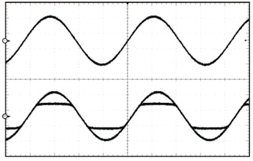
The PLIMIT operation will, if selected, limit the output voltage level to a voltage level below the supply rail. In this case, the amplifier operates as if it was powered by a lower supply voltage, and thereby limiting the output power by voltage clipping. PLIMIT threshold is set by the PLIMIT pin voltage.
 Figure 16. PLIMIT Circuit Operation
 The PLIMIT circuit sets a limit on the output peak-to-peak voltage. The limiting is done by limiting the duty cycle to a fixed maximum value. The limit can be thought of as a "virtual" voltage rail which is lower than the supply connected to PVCC. The "virtual" rail is approximately four times the voltage at the PLIMIT pin. The output voltage can be used to calculate the maximum output power for a given maximum input voltage and speaker impedance.

where
- POUT (10%THD) = 1.25 × POUT (unclipped)
- RL is the load resistance.
- RS is the total series resistance including RDS(on), and output filter resistance.
- VP is the peak amplitude, which is limited by "virtual" voltage rail.