SLOS810A October 2019 – August 2020 TPA3139D2
PRODUCTION DATA
- 1 Features
- 2 Applications
- 3 Description
- 4 Revision History
- 5 Pin Configuration and Functions
- 6 Specifications
-
7 Detailed Description
- 7.1 Overview
- 7.2 Functional Block Diagram
- 7.3
Feature Description
- 7.3.1 Analog Gain
- 7.3.2 SD/ FAULT and MUTE Operation
- 7.3.3 PLIMIT
- 7.3.4 Spread Spectrum and De-Phase Control
- 7.3.5 GVDD Supply
- 7.3.6 DC Detect
- 7.3.7 PBTL Select
- 7.3.8 Short-Circuit Protection and Automatic Recovery Feature
- 7.3.9 Over-Temperature Protection (OTP)
- 7.3.10 Over-Voltage Protection (OVP)
- 7.3.11 Under-Voltage Protection (UVP)
- 7.4 Device Functional Modes
-
8 Application and Implementation
- 8.1 Application Information
- 8.2
Typical Applications
- 8.2.1 Design Requirements
- 8.2.2
Detailed Design Procedure
- 8.2.2.1 Ferrite Bead Filter Considerations
- 8.2.2.2 Efficiency: LC Filter Required with the Traditional Class-D Modulation Scheme
- 8.2.2.3 When to Use an Output Filter for EMI Suppression
- 8.2.2.4 Input Resistance
- 8.2.2.5 Input Capacitor, Ci
- 8.2.2.6 BSN and BSP Capacitors
- 8.2.2.7 Differential Inputs
- 8.2.2.8 Using Low-ESR Capacitors
- 8.2.3 Application Performance Curves
- 9 Power Supply Recommendations
- 10Layout
- 11Device and Documentation Support
Package Options
Mechanical Data (Package|Pins)
- RGE|24
Thermal pad, mechanical data (Package|Pins)
- RGE|24
Orderable Information
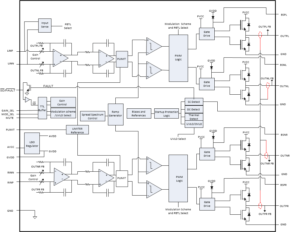
7.2 Functional Block Diagram
