SLOS810A October   2019  – August 2020 TPA3139D2

PRODUCTION DATA  

  1. Features
  2. Applications
  3. Description
  4. Revision History
  5. Pin Configuration and Functions
    1.     Pin Functions
  6. Specifications
    1. 6.1 Absolute Maximum Ratings
    2. 6.2 ESD Ratings
    3. 6.3 Recommended Operating Conditions
    4. 6.4 Thermal Information
    5. 6.5 Electrical Characteristics
    6. 6.6 Switching Characteristics
    7. 6.7 Typical Characteristics,
      1. 6.7.1 Bridge -Tied Load (BTL)
      2. 6.7.2 Paralleled Bridge -Tied Load (PBTL)
  7. Detailed Description
    1. 7.1 Overview
    2. 7.2 Functional Block Diagram
    3. 7.3 Feature Description
      1. 7.3.1  Analog Gain
      2. 7.3.2  SD/ FAULT and MUTE Operation
      3. 7.3.3  PLIMIT
      4. 7.3.4  Spread Spectrum and De-Phase Control
      5. 7.3.5  GVDD Supply
      6. 7.3.6  DC Detect
      7. 7.3.7  PBTL Select
      8. 7.3.8  Short-Circuit Protection and Automatic Recovery Feature
      9. 7.3.9  Over-Temperature Protection (OTP)
      10. 7.3.10 Over-Voltage Protection (OVP)
      11. 7.3.11 Under-Voltage Protection (UVP)
    4. 7.4 Device Functional Modes
      1. 7.4.1 MODE_SEL = LOW: BD Modulation
      2. 7.4.2 MODE_SEL = HIGH: Low-Idle-Current 1SPW Modulation
  8. Application and Implementation
    1. 8.1 Application Information
    2. 8.2 Typical Applications
      1. 8.2.1 Design Requirements
        1. 8.2.1.1 PCB Material Recommendation
        2. 8.2.1.2 PVCC Capacitor Recommendation
        3. 8.2.1.3 Decoupling Capacitor Recommendations
      2. 8.2.2 Detailed Design Procedure
        1. 8.2.2.1 Ferrite Bead Filter Considerations
        2. 8.2.2.2 Efficiency: LC Filter Required with the Traditional Class-D Modulation Scheme
        3. 8.2.2.3 When to Use an Output Filter for EMI Suppression
        4. 8.2.2.4 Input Resistance
        5. 8.2.2.5 Input Capacitor, Ci
        6. 8.2.2.6 BSN and BSP Capacitors
        7. 8.2.2.7 Differential Inputs
        8. 8.2.2.8 Using Low-ESR Capacitors
      3. 8.2.3 Application Performance Curves
        1. 8.2.3.1 EN55013 Radiated Emissions Results
        2. 8.2.3.2 EN55022 Conducted Emissions Results
  9. Power Supply Recommendations
    1. 9.1 Power Supply Decoupling, CS
  10. 10Layout
    1. 10.1 Layout Guidelines
    2. 10.2 Layout Example
  11. 11Device and Documentation Support
    1. 11.1 Device Support
      1. 11.1.1 Third-Party Products Disclaimer
    2. 11.2 Documentation Support
      1. 11.2.1 Related Documentation
    3. 11.3 Receiving Notification of Documentation Updates
    4. 11.4 Support Resources
    5. 11.5 Trademarks
    6. 11.6 Electrostatic Discharge Caution
    7. 11.7 Glossary

Package Options

Mechanical Data (Package|Pins)
Thermal pad, mechanical data (Package|Pins)
Orderable Information

Bridge -Tied Load (BTL)

All measurements taken at audio frequency = 1 kHz, closed-loop gain = 26 dB, BD Modulation, 10 µH + 0.68 µF, TA = 25°C, AES17 measurement filter, unless otherwise noted.
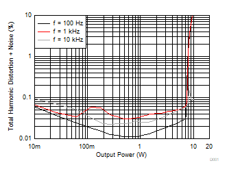
All measurements taken at audio frequency = 1 kHz, closed-loop gain = 26 dB, BD Modulation, 10 µH + 0.68 µF, TA = 25°C, AES17 measurement filter, unless otherwise noted.GUID-184D4622-A23D-4737-81F4-E19F2592D96F-low.gif
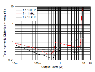
AVCC = PVCC = 12 V, Load = 8 Ω, LC Filter
Figure 6-1 THD+N vs Power (BTL). All measurements taken at audio frequency = 1 kHz, closed-loop gain = 26 dB, BD Modulation, 10 µH + 0.68 µF, TA = 25°C, AES17 measurement filter, unless otherwise noted.
GUID-16E7E134-449B-457D-94F5-9BC2C8E7E580-low.gif
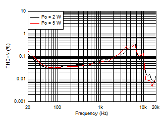
AVCC = PVCC = 12 V, Load = 8 Ω, LC Filter
Figure 6-3 THD+N vs Frequency (BTL)
GUID-A2443FFA-650F-4669-B93B-44086CAEC38D-low.gif
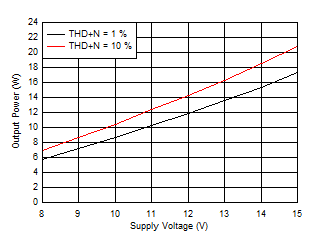
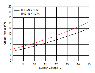
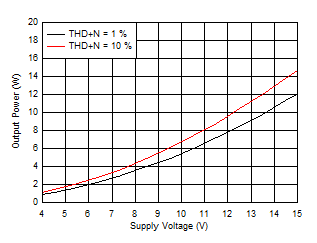
Load = 4 Ω
Figure 6-5 Output Power vs Supply Voltage (BTL)
GUID-4665680B-4FF2-4986-8DE7-98FBBEC93EA4-low.gif
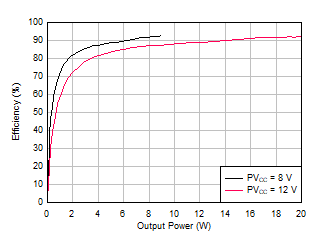
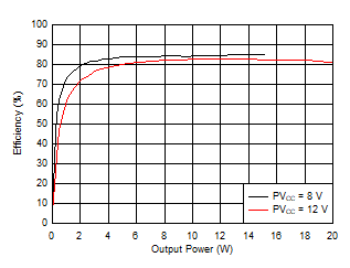
Load = 4 Ω
Figure 6-7 Efficiency vs Output Power (BTL)
GUID-03EBB003-A062-4651-A287-93A4BE60AE77-low.gif
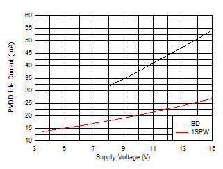
Load = 8 Ω, 1SPW and BD
Figure 6-9 Idle Power vs Supply Voltage (BTL)
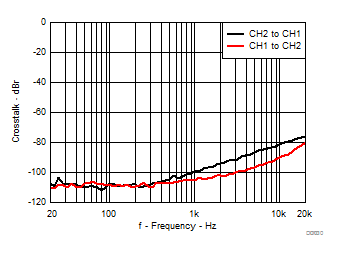
GUID-0B888DC9-4178-4AF5-8AB3-F8277872BE01-low.gif
AVCC=PVCC = 12 V, 1 WLoad = 6 Ω + 47 µH
Figure 6-11 Crosstalk vs Frequency (BTL)
GUID-1E591E6E-A01F-418E-94D9-244037FC6D51-low.gif
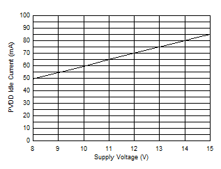
Load = 8 ΩFerrite Bead Filter
Figure 6-13 Idle Current vs Supply Voltage, 8 Ω
GUID-38EAD6A3-7905-4DB8-A535-F2653390D3B5-low.gif
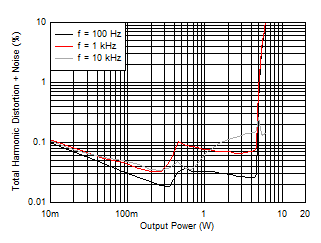
AVCC=PVCC = 7.4 VLoad = 4 Ω1SPW
Figure 6-15 THD+N vs Output Power, 4 Ω
GUID-5759E63E-3BD1-45BD-A5AC-E4DB0A8E47D2-low.gif
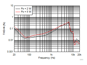
AVCC=PVCC = 12 VLoad = 4 Ω1SPW
Figure 6-17 THD+N vs Frequency, 4 Ω
GUID-940953A0-9ABF-49F8-ABD5-8DD4228D5A63-low.gif
Load = 4 Ω , 1SPW
Figure 6-19 Output Power vs Supply Voltage, 4 Ω
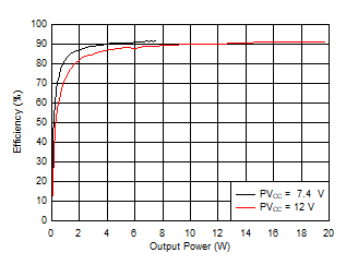
GUID-705F8DB9-4EFB-4CCC-8BCD-058512817B9F-low.gif
Load = 8 Ω , 1SPW
Figure 6-21 Efficiency vs Output Power, 8 Ω
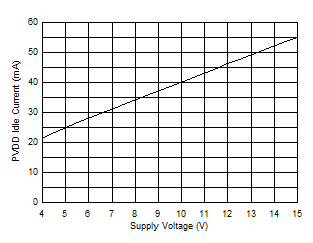
GUID-C4250646-B9E1-49F1-A620-A535DCDDFD77-low.gif
Load = 8 ΩFerrite Bead Filter1SPW
Figure 6-23 Idle Current vs Supply Voltage
GUID-E42919A5-5FF5-4BAA-AF7A-EBC77C46B963-low.gif
AVCC=PVCC = 8 V, Load = 4 Ω, LC Filter
Figure 6-2 THD+N vs Power (BTL)
GUID-D5C50284-956F-48BA-8F7B-7B437B0030CB-low.gif
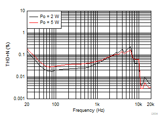
AVCC=PVCC = 12 V, Load = 4 Ω
Figure 6-4 THD+N vs Frequency (BTL)
GUID-E51C1A95-21AF-425C-9266-018DFE60B43B-low.gif
Load = 8 Ω
Figure 6-6 Output Power vs Supply Voltage (BTL)
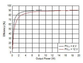
GUID-FE9BA383-64FC-4FCC-86E9-5FE9600B1BA9-low.gif
Load = 8 Ω
Figure 6-8 Efficiency vs Output Power (BTL)
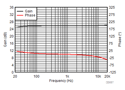
GUID-4F70052C-46FD-4D0D-A93E-EA0901973F73-low.gif
AVCC= PVCC = 12 VLoad = 6 Ω + 47 µH
Figure 6-10 Gain and Phase vs Frequency (BTL)
GUID-9B5624F9-85DD-444A-B6A3-E72BFFB6A06C-low.gif
Load = 8 ΩFerrite Bead Filter
Figure 6-12 Efficiency vs Output Power, 8 Ω
GUID-7F190DF0-7457-4FB6-982B-B5F104355721-low.gif
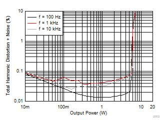
AVCC=PVCC = 12 V, 1 WLoad = 8 Ω1SPW
Figure 6-14 THD+N vs Output Power, 8 Ω
GUID-78737317-736A-4385-8CBC-1F6C6998884F-low.gif
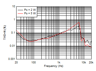
AVCC=PVCC = 12 VLoad = 8 Ω1SPW
Figure 6-16 THD+N vs Frequency, 8 Ω
GUID-4D979BFA-7551-4F2F-9392-6BF4D2A0C9E1-low.gif
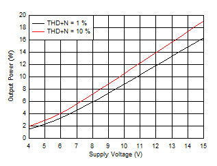
Load = 8 Ω, 1SPW
Figure 6-18 Output Power vs Supply Voltage, 8 Ω
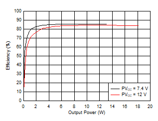
GUID-88BFFDE3-B473-4184-ABA3-C3B1BA492D2B-low.gif
Load = 4 Ω, 1SPW
Figure 6-20 Efficiency vs Output Power, 4 Ω
GUID-EE7E377D-BF33-499B-AF60-A71FD81F19BF-low.gif
Load = 8 Ω,Ferrite Bead Filte1SPW
Figure 6-22 Output Power vs Supply Voltage, 8 Ω