SLOS810A October 2019 – August 2020 TPA3139D2
PRODUCTION DATA
- 1 Features
- 2 Applications
- 3 Description
- 4 Revision History
- 5 Pin Configuration and Functions
- 6 Specifications
-
7 Detailed Description
- 7.1 Overview
- 7.2 Functional Block Diagram
- 7.3
Feature Description
- 7.3.1 Analog Gain
- 7.3.2 SD/ FAULT and MUTE Operation
- 7.3.3 PLIMIT
- 7.3.4 Spread Spectrum and De-Phase Control
- 7.3.5 GVDD Supply
- 7.3.6 DC Detect
- 7.3.7 PBTL Select
- 7.3.8 Short-Circuit Protection and Automatic Recovery Feature
- 7.3.9 Over-Temperature Protection (OTP)
- 7.3.10 Over-Voltage Protection (OVP)
- 7.3.11 Under-Voltage Protection (UVP)
- 7.4 Device Functional Modes
-
8 Application and Implementation
- 8.1 Application Information
- 8.2
Typical Applications
- 8.2.1 Design Requirements
- 8.2.2
Detailed Design Procedure
- 8.2.2.1 Ferrite Bead Filter Considerations
- 8.2.2.2 Efficiency: LC Filter Required with the Traditional Class-D Modulation Scheme
- 8.2.2.3 When to Use an Output Filter for EMI Suppression
- 8.2.2.4 Input Resistance
- 8.2.2.5 Input Capacitor, Ci
- 8.2.2.6 BSN and BSP Capacitors
- 8.2.2.7 Differential Inputs
- 8.2.2.8 Using Low-ESR Capacitors
- 8.2.3 Application Performance Curves
- 9 Power Supply Recommendations
- 10Layout
- 11Device and Documentation Support
Package Options
Mechanical Data (Package|Pins)
- RGE|24
Thermal pad, mechanical data (Package|Pins)
- RGE|24
Orderable Information
3 Description
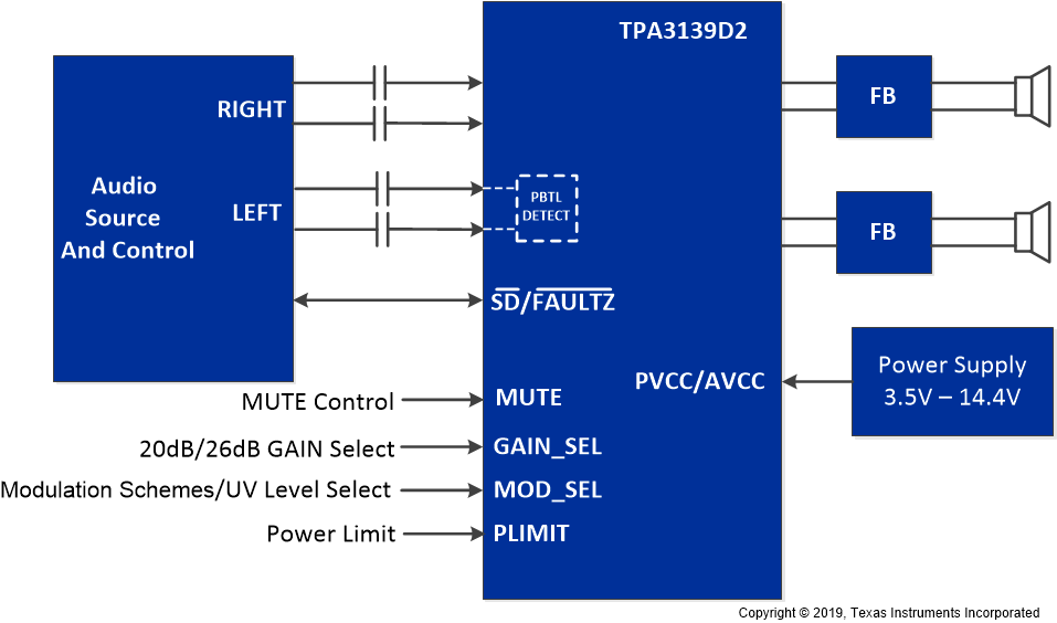
The TPA3139D2 is a 10-W stereo Class-D audio amplifier, featuring a fast turn-on time of <15 ms and mute function. It consumes low idle current of only 20-mA (12-V) and can operate down to 3.5-V, allowing for longer audio playback. Along with a small, 4 x 4 mm2 QFN package, the TPA3139D2 is optimized for 2-cell or 3-cell battery-powered systems with the space constraints. In addition, the Spread Spectrum Control enables the use of inexpensive ferrite bead filters while meeting EMC requirements for system cost reduction.
To further simplify the design, the TPA3139D2 integrates essential protection features including undervoltage, overvoltage, power limit, short circuit, overtemperature, as well as DC speaker protection. All of these protections support automatic recovery.
| PART NUMBER | PACKAGE | BODY SIZE (NOM) |
|---|---|---|
| TPA3139D2 | VQFN (24) | 4.0 mm × 4.0 mm |
 Simplified Schematic