SLOS882B January 2015 – December 2017 TPA3140D2
PRODUCTION DATA.
- 1 Features
- 2 Applications
- 3 Description
- 4 Revision History
- 5 Device Comparison Table
- 6 Pin Configuration and Functions
- 7 Specifications
- 8 Parameter Measurement Information
-
9 Detailed Description
- 9.1 Overview
- 9.2 Functional Block Diagram
- 9.3
Feature Description
- 9.3.1 Gain Setting via GAIN Pin
- 9.3.2 SD Operation
- 9.3.3 Gain Limit Control, LIMTHRES and LIMRATE
- 9.3.4 SPEAKERGUARD Automatic Gain Limit, AGL
- 9.3.5 Thermal Foldback, TFB
- 9.3.6 PLIMIT
- 9.3.7 LIMTHRES
- 9.3.8 Spread Spectrum and De-Phase Control
- 9.3.9 GVDD Supply
- 9.3.10 DC Detect
- 9.3.11 PBTL Select
- 9.3.12 Short-Circuit Protection and Automatic Recovery Feature
- 9.3.13 Thermal Protection
- 9.4 Device Functional Modes
-
10Application and Implementation
- 10.1 Application Information
- 10.2
Typical Applications
- 10.2.1 Design Requirements
- 10.2.2
Detailed Design Procedure
- 10.2.2.1 Ferrite Bead Filter Considerations
- 10.2.2.2 Efficiency: LC Filter Required with the Traditional Class-D Modulation Scheme
- 10.2.2.3 When to Use an Output Filter for EMI Suppression
- 10.2.2.4 Input Resistance
- 10.2.2.5 Input Capacitor, Ci
- 10.2.2.6 BSN and BSP Capacitors
- 10.2.2.7 Differential Inputs
- 10.2.2.8 Using Low-ESR Capacitors
- 10.2.3 Application Performance Curves
- 11Power Supply Recommendations
- 12Layout
- 13Device and Documentation Support
- 14Mechanical, Packaging, and Orderable Information
Package Options
Mechanical Data (Package|Pins)
- PWP|28
Thermal pad, mechanical data (Package|Pins)
- PWP|28
Orderable Information
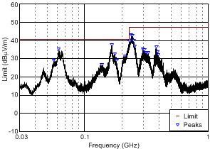
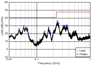
10.2.3.1 EN55013 Radiated Emissions Results
TPA3140D2 EVM, PVCC = 12 V, 8-Ω load, up to 1 meter speaker cable, Spread Spectrum enabled, PO = 1.25 W
| CISPR Class B 3m 30-1000MHz Scan#7- TPA3140D2 EVM with 8R Load, Different ferrite choke, Murata 601FB+1nF, 1-meter cable, Battery supply, SS-TRI, BD, 1.25W, Spkr Wire Config2 |

| CISPR Class B 3m 30-1000MHz Scan#7- TPA3140D2 EVM with 8R Load, Different ferrite choke, Murata 601FB+1nF, 1-meter cable, Battery supply, SS-TRI, BD, 1.25W, Spkr Wire Config2 |
Table 6. Radiated Emission - Horizontal
| FREQUENCY MHz | LIMIT dBµV/m | PEAKS dBµV/m | Q-PEAK dBµV/m | MARGIN dB | TURN TABLE DEGREES | TOWER cm |
|---|---|---|---|---|---|---|
| 166.246 | 40.457 | 21.781 | 21.975 | –18.482 | 44.9 | 100 |
| 237.372 | 47.457 | 29.330 | 29.186 | –18.271 | 326.9 | 100 |
space
Table 7. Radiated Emission - Vertical
| FREQUENCY MHz | LIMIT dBµV/m | PEAKS dBµV/m | Q-PEAK dBµV/m | MARGIN dB | TURN TABLE DEGREES | TOWER cm |
|---|---|---|---|---|---|---|
| 56.841 | 40.457 | 26.213 | 27.058 | –13.399 | 54 | 100 |
| 241.9 | 47.457 | 19.429 | 20.430 | –27.027 | –0.1 | 100 |