SLOS821B June 2013 – September 2014 TPA6133A2
PRODUCTION DATA.
- 1 Features
- 2 Applications
- 3 Description
- 4 Simplified Application Diagram
- 5 Revision History
- 6 Pin Configuration and Functions
- 7 Specification
- 8 Detailed Description
- 9 Application and Implementation
- 10Power Supply Recommendations
- 11Layout
- 12Device and Documentation Support
- 13Mechanical, Packaging, and Orderable Information
Package Options
Mechanical Data (Package|Pins)
- RTJ|20
Thermal pad, mechanical data (Package|Pins)
- RTJ|20
Orderable Information
8 Detailed Description
8.1 Overview
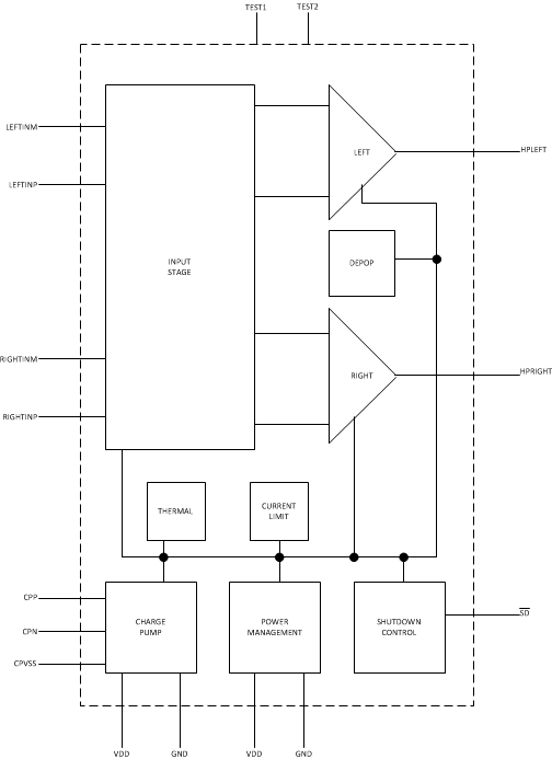
Headphone channels and the charge pump are activated by asserting the SD pin to logic 1. The charge pump generates a negative supply voltage for the output amplifiers. This allows a 0 V bias at the outputs, eliminating the need for bulky output capacitors. The thermal block detects faults and shuts down the device before damage occurs. The current limit block prevents the output current from getting high enough to damage the device. The De-Pop block eliminates audible pops during power-up, power-down, and amplifier enable and disable events.
8.2 Functional Block Diagram

8.3 Feature Description
8.3.1 Headphone Amplifiers
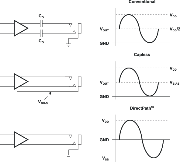
Single-supply headphone amplifiers typically require dc-blocking capacitors. The capacitors are required because most headphone amplifiers have a dc bias on the outputs pin. If the dc bias is not removed, power consumption will be higher, and large amounts of dc current rush through the headphones, potentially damaging them. The top drawing in Figure 19 illustrates the conventional headphone amplifier connection to the headphone jack and output signal.
DC blocking capacitors are often large in value. The headphone speakers (typical resistive values of 16 Ω or 32 Ω) combine with the dc blocking capacitors to form a high-pass filter. Equation 1 shows the relationship between the load impedance (RL), the capacitor (CO), and the cutoff frequency (fC).

CO can be determined using Equation 2, where the load impedance and the cutoff frequency are known.

If fc is low, the capacitor must then have a large value because the load resistance is small. Large capacitance values require large package sizes. Large package sizes consume PCB area, stand high above the PCB, increase cost of assembly, and can reduce the fidelity of the audio output signal.
Two different headphone amplifier applications are available that allow for the removal of the output dc blocking capacitors. The capless amplifier architecture is implemented in the same manner as the conventional amplifier with the exception of the headphone jack shield pin. This amplifier provides a reference voltage, which is connected to the headphone jack shield pin. This is the voltage on which the audio output signals are centered. This voltage reference is half of the amplifier power supply to allow symmetrical swing of the output voltages. Do not connect the shield to any GND reference or large currents will result. The scenario can happen if, for example, an accessory other than a floating GND headphone is plugged into the headphone connector. See the second block diagram and waveform in Figure 19.
 Figure 19. Amplifier Applications
The DirectPath™ amplifier architecture operates from a single supply but makes use of an internal charge pump to provide a negative voltage rail. Combining the user provided positive rail and the negative rail generated by the IC, the device operates in what is effectively a split supply mode. The output voltages are now centered at zero volts with the capability to swing to the positive rail or negative rail. The DirectPath™ amplifier requires no output dc blocking capacitors, and does not place any voltage on the sleeve. The bottom block diagram and waveform of Figure 19 illustrate the ground-referenced headphone architecture. This is the architecture of the TPA6133A2.
8.4 Device Functional Modes
8.4.1 Modes of Operation
The TPA6133A2 supports two modes of operation. When the SD pin is driven to logic 0, the device is in low power mode where the charge pump is powered down, the headphone channel is disabled and the outputs are pulled to ground. When the SD pin is driven to logic 1, the device enters an active mode with charge pump powered up and headphone channel enabled with channel gain of +4dB. The transition from inactive to active and active to inactive states is done softly to avoid audible artifacts.