SLOS490C July 2006 – November 2015
PRODUCTION DATA.
- 1 Features
- 2 Applications
- 3 Description
- 4 Revision History
- 5 Device Comparison Table
- 6 Pin Configuration and Functions
- 7 Specifications
- 8 Parameter Measurement Information
- 9 Detailed Description
- 10Application and Implementation
- 11Power Supply Recommendations
- 12Layout
- 13Device and Documentation Support
- 14Mechanical, Packaging, and Orderable Information
Package Options
Mechanical Data (Package|Pins)
Thermal pad, mechanical data (Package|Pins)
Orderable Information
12 Layout
12.1 Layout Guidelines
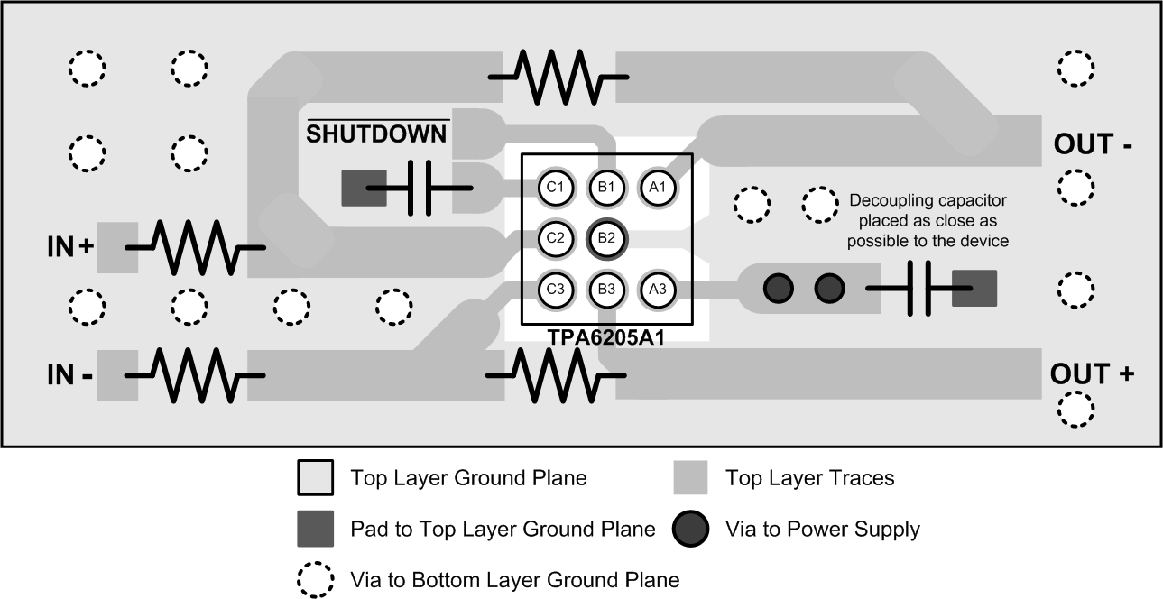
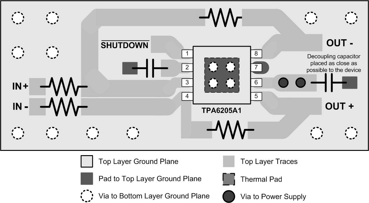
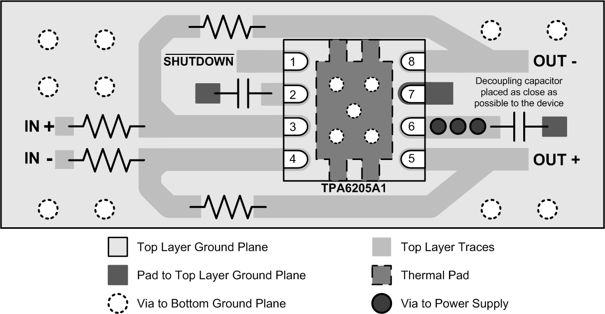
Placing the decoupling capacitors as close as possible to the device is important for the efficiency of the class-D amplifier. Any resistance or inductance in the trace between the device and the capacitor can cause a loss in efficiency.
For the DRB (QFN/SON) and DGN (MSOP) to presence of voids within the exposed thermal pad interconnection. Total elimination is difficult, but the design of the exposed pad stencil is key. The stencil design proposed in the Texas Instruments application note QFN/SON PCB Attachment (SLUA271) enables out-gassing of the solder paste during reflow as well as regulating the finished solder thickness. Typically the solder paste coverage is approximately 50% of the pad area.
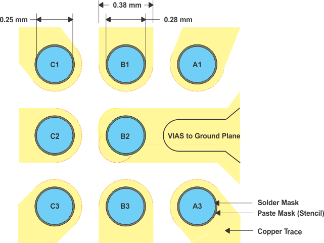
In making the pad size for the BGA balls, it is recommended that the layout use soldermask-defined (SMD) land. With this method, the copper pad is made larger than the desired land area, and the opening size is defined by the opening in the solder mask material. The advantages normally associated with this technique include more closely controlled size and better copper adhesion to the laminate. Increased copper also increases the thermal performance of the IC. Better size control is the result of photo imaging the stencils for masks. Small plated vias should be placed near the center ball connecting ball B2 to the ground plane. Added plated vias and ground plane act as a heatsink and increase the thermal performance of the device. Figure 38 shows the appropriate diameters for a 2 mm × 2 mm MicroStar Junior™ BGA layout.
It is very important to keep the TPA6205A1 external components very close to the TPA6205A1 to limit noise pickup. The TPA6205A1 layout is shown in the next section as a layout example.
 Figure 38. MicroStar Junior™ BGA Recommended Layout
12.2 Layout Example
 Figure 39. TPA6205A1 BGA Layout
 Figure 40. TPA6205A1 HVSSOP Layout
 Figure 41. TPA6205A1 VSON Layout