SLLSE96F September 2011 – October 2015 TPD12S016
PRODUCTION DATA.
- 1 Features
- 2 Applications
- 3 Description
- 4 Revision History
- 5 Pin Configuration and Functions
- 6 Specifications
-
7 Detailed Description
- 7.1 Overview
- 7.2 Functional Block Diagram
- 7.3
Feature Description
- 7.3.1 Conforms to HDMI Compliance Tests Without any External Components
- 7.3.2 IEC 61000-4-2 ESD Protection
- 7.3.3 Supports HDMI 1.4 Data Rate
- 7.3.4 Matches Class D and Class C Pin Mapping
- 7.3.5 8-Channel ESD Lines for Four Differential Pairs with Ultra-low Differential Capacitance Matching (0.05 pF)
- 7.3.6 On-Chip Load Switch With 55-mA Current Limit Feature at the HDMI 5V_OUT Pin
- 7.3.7 Auto-direction Sensing I2C Level Shifter With One-Shot Circuit to Drive a Long HDMI Cable (750-pF Load)
- 7.3.8 Back-Drive Protection on HDMI Connector Side Ports
- 7.3.9 Integrated Pullup and Pulldown Resistors per HDMI Specification
- 7.3.10 Space Saving 24-Pin RKT Package and 24-TSSOP Package
- 7.3.11 DDC/CEC LEVEL SHIFT Circuit Operation
- 7.3.12 DDC/CEC Level Shifter Operational Notes For VCCA = 1.8 V
- 7.3.13 Rise-Time Accelerators
- 7.3.14 Noise Considerations
- 7.3.15 Resistor Pullup Value Selection
- 7.4 Device Functional Modes
- 8 Application and Implementation
- 9 Power Supply Recommendations
- 10Layout
- 11Device and Documentation Support
- 12Mechanical, Packaging, and Orderable Information
Package Options
Refer to the PDF data sheet for device specific package drawings
Mechanical Data (Package|Pins)
- RKT|24
- PW|24
Thermal pad, mechanical data (Package|Pins)
- RKT|24
Orderable Information
8 Application and Implementation
NOTE
Information in the following applications sections is not part of the TI component specification, and TI does not warrant its accuracy or completeness. TI’s customers are responsible for determining suitability of components for their purposes. Customers should validate and test their design implementation to confirm system functionality.
8.1 Application Information
TPD12S016 provides IEC 61000-4-2 Level 4 Contact ESD rating to the HDMI 1.4 transmitter port. Buffered VLT's translate DDC and CEC channels bidirectionally. The system is designed to work properly with no external pullup resistors on the DDC, CEC, and HPD lines. The CEC line has an integrated 3.3-V rail, eliminating the need for a 3.3-V supply on board.
8.2 Typical Application
The TPD12S016 is placed as close as possible to the HDMI connector to provide voltage level translation, 5V_OUT current limiting and overall ESD protection for the HDMI controller.
8.2.1 Example 1: HDMI Controller Using One Control Line
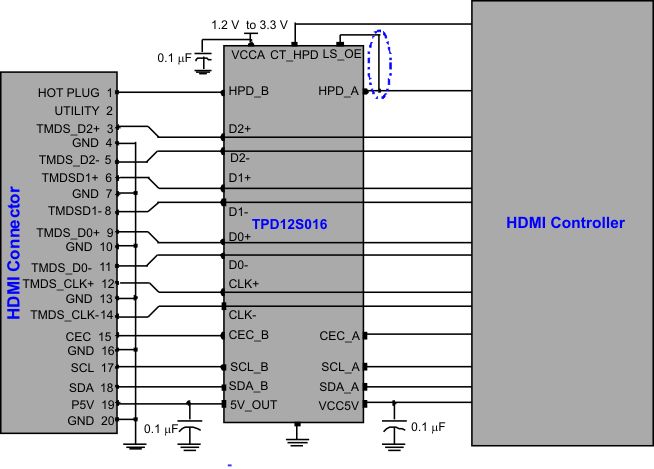
In the example shown in Figure 15, the HDMI driver chip is controlling the TPD12S016 through only one control line, CT_HPD. In this mode the HPD_A to LS_OE pin are connected as shown in the oval dotted line of Figure 15. To fully enable TPD12S016, set CT_HPD above VIH. To fully disable TPD12S016, set CT_HPD below VIL.
 Figure 15. TPD12S016 with an HDMI Controller Using One GPIO for HDMI Interface Control
8.2.1.1 Design Requirements
For this example, use the following table as input parameters:
Table 2. HDMI Controller Using One Control Line Design Parameters
| DESIGN PARAMETERS | EXAMPLE VALUE | ||
|---|---|---|---|
| Voltage on VCCA | 1.8 V | ||
| Voltage on VCC5V | 5.0 V | ||
| Drive CT_HPD low (disabled) | –0.5 V to 0.4 V | ||
| Drive CT_HPD high (enabled) | 1.0 V to 1.8 V | ||
| Drive a logical 1 | A to B | SCL and SDA | 1.26 V to 1.8 V |
| CEC | |||
| B to A | SCL and SDA | 3.5 V to 5.0 V | |
| CEC | 2.31 V to 3.3 V | ||
| Drive a logical 0 | A to B | SCL and SDA | –0.5 V to 0.117 V |
| CEC | |||
| B to A | SCL and SDA | –0.5 V to 1.5 V | |
| CEC | –0.5 V to 0.99 V | ||
8.2.1.2 Detailed Design Procedure
To begin the design process, the designer needs to know the VCC5V voltage range and the logic level, VCCA, voltage range.
8.2.2 Example 2: HDMI Controller Using CT_HPD and LS_OE
Some HDMI driver chips may have two GPIOs to control the HDMI interface chip. In this case a flexible power saving mode can be implemented. The load switch can be activated by CT_HPD while the level shifters are inactive, using LS_OE. This results in TPD12S016 drawing only approximately 30 µA, a reduction of 170 µA from being fully on. After a hot plug is detected, the HDMI controller can enable the rest of the HDMI interface chip using LS_OE.
 Figure 18. TPD12S016 with an HDMI Controller Using Two GPIOs For HDMI Interface Control
8.2.2.1 Design Requirements
For this example, use Table 3 for input parameters:
Table 3. HDMI Controller Using CT_HPD and LS_OE Design Parameters
| DESIGN PARAMETERS | EXAMPLE VALUE | ||
|---|---|---|---|
| Voltage on VCCA | 3.3 V | ||
| Voltage on VCC5V | 5.0 V | ||
| Drive CT_HPD low (disabled) | –0.5 V to 0.4 V | ||
| Drive LS_OE low (disabled) | |||
| Drive CT_HPD high (enabled) | 1.0 V to 3.3 V | ||
| Drive LS_OE high (enabled) | |||
| Drive a logical 1 | A to B | SCL and SDA | 2.31 V to 3.3 V |
| CEC | |||
| B to A | SCL and SDA | 3.5 V to 5.0 V | |
| CEC | 2.31 V to 3.3 V | ||
| Drive a logical 0 | A to B | SCL and SDA | –0.5 V to 0.214 V |
| CEC | |||
| B to A | SCL and SDA | –0.5 V to 1.5 V | |
| CEC | –0.5 V to 0.99 V | ||
8.2.2.2 Detailed Design Procedure
To begin the design process, the designer needs to know the VCC5V voltage range and the logic level, VCCA, voltage range.
8.2.2.3 Application Curves
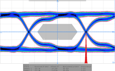
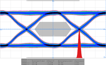
Refer to Application Curves for related application curves.

