SLVS640F October 2007 – February 2015 TPD12S520
PRODUCTION DATA.
- 1 Features
- 2 Applications
- 3 Description
- 4 Revision History
- 5 Pin Configuration and Functions
- 6 Specifications
-
7 Detailed Description
- 7.1 Overview
- 7.2 Functional Block Diagram
- 7.3
Feature Description
- 7.3.1 ±8-kV Contact ESD Protection on External Lines
- 7.3.2 Single-Chip ESD Solution for HDMI Driver
- 7.3.3 Supports All HDMI 1.3 and HDMI 1.4b Data Rates
- 7.3.4 38-Pin TSSOP Provides Seamless Layout Option With HDMI Connector
- 7.3.5 24-Pin WQFNPackage for Space Constrained Applications
- 7.3.6 Integrated Level Shifting for the Control Lines
- 7.3.7 Backdrive Protection
- 7.3.8 Lead-Free Package
- 7.4 Device Functional Modes
- 8 Application and Implementation
- 9 Power Supply Recommendations
- 10Layout
- 11Device and Documentation Support
- 12Mechanical, Packaging, and Orderable Information
Package Options
Mechanical Data (Package|Pins)
Thermal pad, mechanical data (Package|Pins)
Orderable Information
1 Features
- IEC 61000-4-2 Level 4 ESD Protection
- Single-Chip ESD Solution for HDMI Driver
- 12 Channel ESD Protection Diodes
- Supports All HDMI 1.3 and HDMI 1.4b Data Rates
(–3 dB Frequency > 3 GHz) - 0.8-pF Capacitance for the High Speed TMDS Lines
- 0.05-pF Matching Capacitance Between the Differential Signal Pair
- 38-Pin TSSOP Provides Seamless Layout Option with HDMI Connector
- 24-Pin WQFN Package for Space Constrained Applications
- Backdrive Protection
- Lead-Free Package
2 Applications
- Video Interface
- Consumer Electronics
- Displays and Digital Televisions
- Handheld Displays
3 Description
The TPD12S520 is a single-chip electro-static discharge (ESD) circuit protection device for the high-definition multimedia interface (HDMI) receiver port. While providing ESD protection with transient voltage suppression (TVS) diodes, the TVS protection adds little or no additional glitch in the high-speed differential signals. The high-speed transition minimized differential signaling (TMDS) ESD protection lines add only 0.8-pF capacitance.
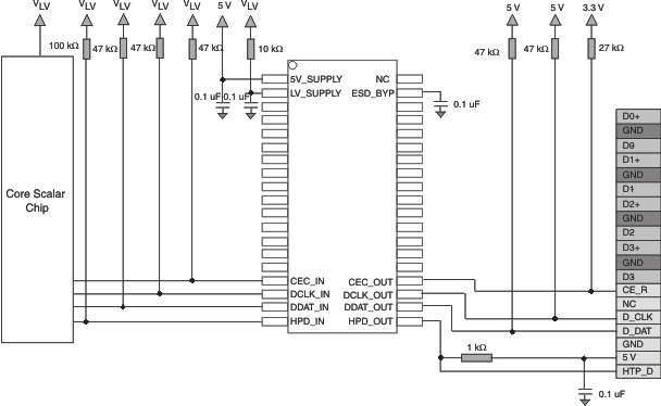
The low-speed control lines offer voltage-level shifting to eliminate the need for an external voltage level-shifter IC. The control line TVS diodes add 3.5-pF capacitance to the control lines. The 38-pin DBT package offers a seamless layout routing option to eliminate the routing glitch for the differential signal pairs. The DBT package pitch (0.5 mm) matches with the HDMI connector pitch. In addition, the pin mapping follows the same order as the HDMI connector pin mapping. This HDMI receiver port protection and interface device is designed specifically for HDMI receiver-interface protection. The 24-pin RMN package offers flow through routing using only two layers for highly integrated, space-efficient full HDMI protection.
Device Information(1)
| DEVICE NAME | PACKAGE | BODY SIZE (NOM) |
|---|---|---|
| TPD12S520 | TSSOP (38) | 6.40 mm × 9.70 mm |
| WQFN (24) | 4.50 mm × 1.50 mm |
- For all available packages, see the orderable addendum at the end of the datasheet.
Circuit Protection Scheme
