SLVS639F October 2007 – February 2016 TPD12S521
PRODUCTION DATA.
- 1 Features
- 2 Applications
- 3 Description
- 4 Circuit Protection Scheme
- 5 Revision History
- 6 Pin Configuration and Functions
- 7 Specifications
-
8 Detailed Description
- 8.1 Overview
- 8.2 Functional Block Diagram
- 8.3
Feature Description
- 8.3.1 Single-Chip ESD Solution for HDMI Driver
- 8.3.2 Supports All HDMI 1.3 and HDMI 1.4b Data Rates
- 8.3.3 Integrated Level Shifting for the Control Lines
- 8.3.4 ±8-kV Contact ESD Protection on External Lines
- 8.3.5 38-Pin TSSOP Provides Seamless Layout Option With HDMI Connector
- 8.3.6 Backdrive Protection
- 8.3.7 Lead-Free Package
- 8.3.8 On-Chip Current Regulator With 55-mA Current Output
- 8.4 Device Functional Modes
- 9 Application and Implementation
- 10Power Supply Recommendations
- 11Layout
- 12Device and Documentation Support
- 13Mechanical, Packaging, and Orderable Information
Package Options
Refer to the PDF data sheet for device specific package drawings
Mechanical Data (Package|Pins)
- DBT|38
Thermal pad, mechanical data (Package|Pins)
Orderable Information
9 Application and Implementation
NOTE
Information in the following applications sections is not part of the TI component specification, and TI does not warrant its accuracy or completeness. TI’s customers are responsible for determining suitability of components for their purposes. Customers should validate and test their design implementation to confirm system functionality.
9.1 Application Information
TPD12S521 provides IEC61000-4-2 Level 4 Contact ESD rating to the HDMI 1.4 transmitter port. Integrated voltage-level shifting reduces the board space needed to implement the control lines.
9.2 Typical Application
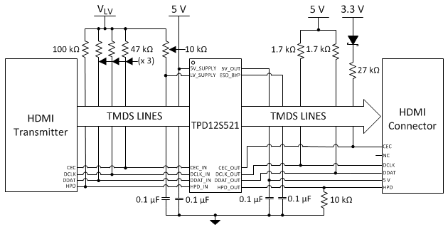
Refer to Figure 2 for a typical schematic for an HDMI 1.4 transmitter port protected with TPD12S521. The eight TMDS data lines (D2+/-, D1+/-, D0+/-, CLK+/-) each have two pins on TPD12S521 to connect to. The TMDS data lines flow through their respective pin pairs, attaching to the passive ESD protection circuitry. To block reverse current to the 3.3-V logic power rail, connect CEC_OUT to the 3.3-V logic level with a 27-kΩ pull-up resistor in series with a Schottky diode.
 Figure 2. TPD12S521 Configured With an HDMI 1.4 Transmitter Port
9.2.1 Design Requirements
For this example, use the following table as input parameters:
| Design Parameters | Example Value |
|---|---|
| Voltage on 5V_SUPPLY | 4.5 V - 5.5 V |
| Voltage on LV_SUPPLY | 1.7 V - 1.9 V |
9.2.2 Detailed Design Procedure
To begin the design process the designer needs to know the 5V_SUPPLY voltage range and the logic level, LV_SUPPLY, voltage range.
9.2.3 Application Curves
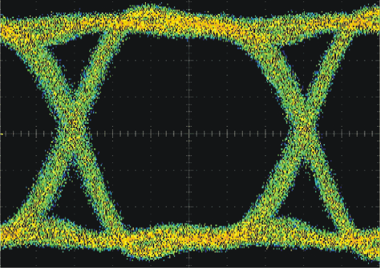
 Figure 3. HDMI 1.65Gbps Eye Diagram With TPD12S521 on a Test Board
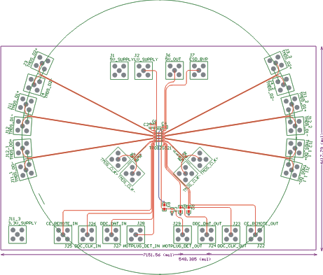
 Figure 5. Test Board to Measure Eye Diagram for the TPD12S521 (Refer to Eye Diagram Plot)
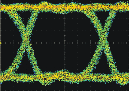
 Figure 4. HDMI 1.65Gbps Eye Diagram Without TPD12S521 on a Test Board