SLVSBO7O December 2012 – August 2024 TPD1E05U06 , TPD4E05U06 , TPD6E05U06
PRODUCTION DATA
- 1
- 1 Features
- 2 Applications
- 3 Description
- 4 Pin Configuration and Functions
- 5 Specifications
- 6 Detailed Description
- 7 Application and Implementation
- 8 Device and Documentation Support
- 9 Revision History
- 10Mechanical, Packaging, and Orderable Information
Package Options
Refer to the PDF data sheet for device specific package drawings
Mechanical Data (Package|Pins)
- DPY|2
- DYA|2
Thermal pad, mechanical data (Package|Pins)
Orderable Information
10.1 Tape and Reel Information

| Device | Package Type |
Package Drawing | Pins | SPQ | Reel Diameter (mm) |
Reel Width W1 (mm) |
A0 (mm) |
B0 (mm) |
K0 (mm) |
P1 (mm) |
W (mm) |
Pin1 Quadrant |
|---|---|---|---|---|---|---|---|---|---|---|---|---|
| TPD1E05U06DPYR | X1SON | DPY | 2 | 10000 | 180.0 | 8.4 | 0.67 | 1.15 | 0.46 | 2.0 | 8.0 | Q2 |
| TPD1E05U06DPYT | X1SON | DPY | 2 | 250 | 180.0 | 9.5 | 0.66 | 1.15 | 0.66 | 2.0 | 8.0 | Q1 |
| TPD1E05U06DYAR | SOT-5X3 | DYA | 2 | 3000 | 178.0 | 9.5 | 0.5 | 1.94 | 0.73 | 2.0 | 8.0 | Q1 |
| TPD4E05U06DQAR | USON | DQA | 10 | 3000 | 180.0 | 8.4 | 1.2 | 2.7 | 0.63 | 4.0 | 8.0 | Q1 |
| TPD6E05U06RVZR | USON | RVZ | 14 | 3000 | 180.0 | 13.2 | 1.65 | 3.8 | 0.7 | 4.0 | 12.0 | Q1 |
| TPD6E05U06RVZR | USON | RVZ | 14 | 3000 | 178.0 | 13.5 | 1.6 | 3.75 | 0.7 | 4.0 | 12.0 | Q1 |
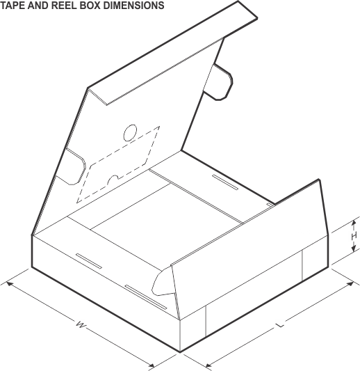
| Device | Package Type | Package Drawing | Pins | SPQ | Length (mm) | Width (mm) | Height (mm) |
|---|---|---|---|---|---|---|---|
| TPD1E05U06DPYR | X1SON | DPY | 2 | 10,000 | 210.000 | 185.000 | 35.000 |
| TPD1E05U06DPYT | X1SON | DPY | 2 | 250 | 184.0 | 184.0 | 19.0 |
| TPD1E05U06DYAR | SOT-5X3 | DYA | 2 | 3000 | 210.0 | 200.0 | 42.0 |
| TPD4E05U06DQAR | USON | DQA | 10 | 3000 | 210.0 | 185.0 | 35.0 |
| TPD6E05U06RVZR | USON | RVZ | 14 | 3000 | 189.0 | 185.0 | 36.0 |
| TPD6E05U06RVZR | USON | RVZ | 14 | 3000 | 184.0 | 184.0 | 19.0 |