-
TPD2E009 2-Channel ESD Solution for High-Speed (6-Gbps) Differential Interface
- 1 Features
- 2 Applications
- 3 Description
- 4 Revision History
- 5 Pin Configuration and Functions
- 6 Specifications
- 7 Detailed Description
- 8 Application and Implementation
- 9 Power Supply Recommendations
- 10Layout
- 11Device and Documentation Support
- 12Mechanical, Packaging, and Orderable Information
- IMPORTANT NOTICE
Package Options
Mechanical Data (Package|Pins)
Thermal pad, mechanical data (Package|Pins)
- DRT|3
Orderable Information
TPD2E009 2-Channel ESD Solution for High-Speed (6-Gbps) Differential Interface
1 Features
- Supports Data Rates up to 6 Gbps
- IEC 61000-4-2 ESD Protection
- ±8-kV Contact Discharge
- ±8-kV Air-Gap Discharge
- IEC 61000-4-5 Surge Protection
- 5 A (8/20 µs)
- Low Capacitance
- DRT: 0.7-pF (Typ)
- DBZ: 0.9-pF (Typ)
- 0.05-pF Matching Capacitance Between the Differential Signal Pair
- Dual-Matching TVS Diodes to Protect the Differential Data and Clock Lines of HDMI, LVDS, SATA, Ethernet, or USB Interfaces
- Space-Saving DRT and DBZ Package Options
- Flow-Through Pin Mapping for the High-Speed Lines Ensures Zero Additional Skew Due to Board Layout While Placing the ESD-Protection Chip Near the Connector
2 Applications
- End Equipment:
- Notebooks
- Set-Top Boxes
- Portable Computers
- DVD Players
- Media Players
- Interfaces:
- HDMI 2.0
- USB 3.0
- eSATA
- Ethernet
3 Description
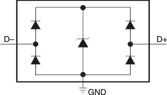
The TPD2E009 device provides two ESD protection diodes with flow-through pin mapping for ease of board layout. This device has been designed to protect sensitive components which are connected to ultra high-speed data and transmission lines. The TPD2E009 offers transient voltage suppression for Level 4 of IEC 61000-4-2 Contact ESD protection. TVS protection up to a 5-A (8/20 μs) peak pulse-current rating per the IEC 61000-4-5 (lightning) specification is also provided.
The monolithic silicon technology allows matching between the differential signal pairs. The less than 0.05-pF differential capacitance ensures that the differential signal distortion due to added ESD circuit protection remains minimal. The low capacitance
(0.7-pF) is suitable for high-speed data rates up to
6 Gbps.
The TPD2E009 TVS diode is offered in a DRT
(1 mm × 0.8 mm) package for space-saving portable applications. The industry standard DBZ (2.92 mm × 1.3 mm) package offers additional flexibility in the board layout for the system designer.
Typical applications for the TPD2E009 line of ESD protection products are: HDMI, USB, eSATA, and ethernet interfaces in notebooks, DVD and media players, set-top boxes, and portable computers.
Device Information(1)
| PART NUMBER | PACKAGE | BODY SIZE (NOM) |
|---|---|---|
| TPD2E009 | SOT (3) | 2.92 mm × 1.30 mm |
| 1.00 mm × 0.80 mm |
- For all available packages, see the orderable addendum at the end of the data sheet.
TPD2E009 Circuit

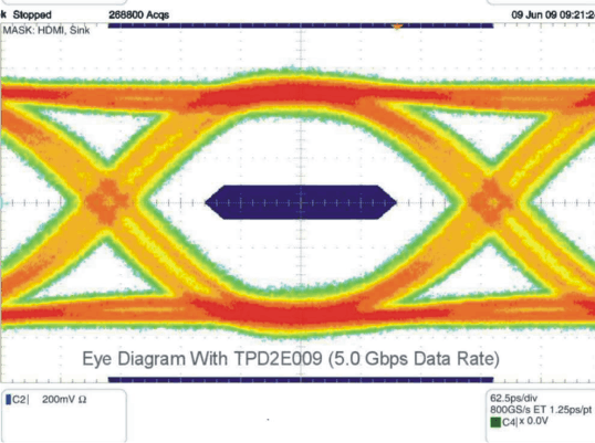
TPD2E009 Application Curve

4 Revision History
Changes from A Revision (June 2009) to B Revision
- Added Pin Configuration and Functions section, ESD Ratings table, Feature Description section, Device Functional Modes, Application and Implementation section, Power Supply Recommendations section, Layout section, Device and Documentation Support section, and Mechanical, Packaging, and Orderable Information section Go
5 Pin Configuration and Functions

Pin Functions
| PIN | TYPE | DESCRIPTION | |
|---|---|---|---|
| NAME | NO. | ||
| D+ | 1 | ESD port | High-speed ESD clamp provides ESD protection to the high-speed differential data lines |
| D– | 2 | ||
| GND | 3 | GND | Ground |
6 Specifications
6.1 Absolute Maximum Ratings(1)
over operating free-air temperature range (unless otherwise noted)| MIN | MAX | UNIT | |||
|---|---|---|---|---|---|
| Operating temperature | –40 | 85 | °C | ||
| I/O voltage tolerance | D+, D– pins | 0 | 6 | V | |
| Peak pulse current (tp = 8/20 μs) | 5 | A | |||
| Peak pulse power (tp = 8/20 μs) | 45 | W | |||
| Storage temperature, Tstg | –65 | 125 | °C | ||
6.2 ESD Ratings
| VALUE | UNIT | ||||
|---|---|---|---|---|---|
| V(ESD) | Electrostatic discharge | Human body model (HBM), per ANSI/ESDA/JEDEC JS-001(1) | ±15000 | V | |
| Charged-device model (CDM), per JEDEC specification JESD22-C101(2) | ±1000 | ||||
| IEC 61000-4-2 contact discharge | D+, D– pins | ±8000 | |||
| IEC 61000-4-2 air-gap discharge | D+, D– pins | ±8000 | |||
6.3 Recommended Operating Conditions
over operating free-air temperature range (unless otherwise noted)| MIN | NOM | MAX | UNIT | ||
|---|---|---|---|---|---|
| Operating free-air temperature, TA | –40 | 85 | °C | ||
| Operating voltage | Pin 1 or 2 to 3 or Pin 3 to 1 or 2 | 0 | 5.5 | V | |
6.4 Thermal Information
| THERMAL METRIC(1) | TPD2E009 | UNIT | ||
|---|---|---|---|---|
| DBZ (SOT) | DRT (SOT) | |||
| 3 PINS | 3 PINS | |||
| RθJA | Junction-to-ambient thermal resistance | 461.8 | 610 | °C/W |
| RθJC(top) | Junction-to-case (top) thermal resistance | 216.2 | 288 | °C/W |
| RθJB | Junction-to-board thermal resistance | 195.6 | 118.4 | °C/W |
| ψJT | Junction-to-top characterization parameter | 70.1 | 20.2 | °C/W |
| ψJB | Junction-to-board characterization parameter | 193.7 | 116.4 | °C/W |
6.5 Electrical Characteristics
over operating free-air temperature range (unless otherwise noted)| PARAMETER | TEST CONDITIONS | MIN | TYP | MAX | UNIT | ||
|---|---|---|---|---|---|---|---|
| VRWM | Reverse stand-off voltage | D+, D– pins to ground | 5.5 | V | |||
| VCLAMP | Clamp voltage | D+, D– pins to ground, | IIO = 1 A | 8 | V | ||
| IIO | Current from I/O port to supply pins | VIO = 2.5 V | 0.01 | 0.1 | μA | ||
| VD | Diode forward voltage | D+, D– pins, lower clamp diode, |
VIO = 2.5 V, ID = 8 mA | 0.6 | 0.8 | 0.95 | V |
| D+, D– pins, upper clamp diode, DRY package |
VCC = 0 V, ID = –8 mA | 0.6 | 0.8 | 0.95 | |||
| RDYN | Dynamic resistance | D+, D– pins, | I = 1 A | 1 | Ω | ||
| CIO | I/O capacitance | D+, D– pins, DBZ Package | VIO = 2.5 V, f = 10 MHz | 0.9 | pF | ||
| D+, D– pins, DRT Package | VIO = 2.5 V, f = 10 MHz | 0.7 | pF | ||||
| VBR | Break-down voltage | IIO = 1 mA | 7 | V | |||
6.6 Typical Characteristics
 Figure 1. I/O Capacitance vs I/O Voltage (TA= 25°C)

(Measured at One I/O, With the Other I/O Open)
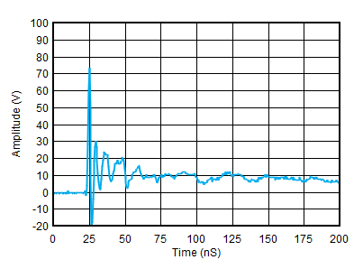
 Figure 5. IEC Clamping Waveforms (8-kV Contact)
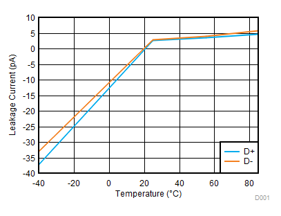
 Figure 2. Leakage Current vs Temperature (VIO = 2.5 V)
 Figure 4. D+, D– Transmission Line Pulser Plot
 (100-ns Pulse, 10-ns Rise Time)
 Figure 6. IEC Clamping Waveforms (–8-kV Contact)