SLVS953B June 2009 – August 2015 TPD2E009
PRODUCTION DATA.
- 1 Features
- 2 Applications
- 3 Description
- 4 Revision History
- 5 Pin Configuration and Functions
- 6 Specifications
- 7 Detailed Description
- 8 Application and Implementation
- 9 Power Supply Recommendations
- 10Layout
- 11Device and Documentation Support
- 12Mechanical, Packaging, and Orderable Information
Package Options
Mechanical Data (Package|Pins)
Thermal pad, mechanical data (Package|Pins)
- DRT|3
Orderable Information
8 Application and Implementation
NOTE
Information in the following applications sections is not part of the TI component specification, and TI does not warrant its accuracy or completeness. TI’s customers are responsible for determining suitability of components for their purposes. Customers should validate and test their design implementation to confirm system functionality.
8.1 Application Information
The TPD2E009 device is a diode-array type TVS typically used to provide a path to ground for dissipating ESD events on high-speed signal lines between a human-interface connector and a system. As the current from ESD passes through the TVS, only a small voltage drop is present across the diode. This is the voltage presented to the protected IC. The low RDYN of the triggered TVS holds this voltage, VCLAMP, to a tolerable level to the protected IC.
8.2 Typical Application
The TPD2E009 device is typically used to protect a single high-speed differential pair. Multiple TPD2E009 devices can be used to provide protection for connectors with multiple differential data lanes. This example is applicable to many interface types including:
- HDMI
- USB
- eSATA
- ethernet interfaces
 Figure 7. TPD2E009 in a High-Speed Interface
8.2.1 Design Requirements
For this design example, TPD2E009 is used to protect any differential data pair meeting the design requirements shown in the following table.
| DESIGN PARAMETER | VALUE |
|---|---|
| Maximum signal range on D+ and D– | 0 V to 5.5 V |
| Maximum Operating Frequency | 3 GHz |
8.2.2 Detailed Design Procedure
To begin the design process, some parameters must be decided upon; the designer must know the following:
- The signal voltage range on the protected lines
- The maximum operating frequency
8.2.3 Application Curves
 Figure 8. Eye Diagram With TPD2E009
 (3.3-Gbps Data Rate)
(3-Pin DBZ Package)
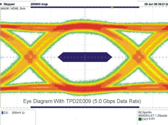
 Figure 10. Eye Diagram With TPD2E009
(5-Gbps Data Rate)
(3-Pin DBZ Package)
 Figure 12. Eye Diagram With TPD2E009
(6-Gbps Data Rate)
(3-Pin DBZ Package)
 Figure 9. Eye Diagram Without TPD2E009
 (3.3-Gbps Data Rate)
(3-Pin DBZ Package)
 Figure 11. Eye Diagram Without TPD2E009
(5-Gbps Data Rate)
(3-Pin DBZ Package)
 Figure 13. Eye Diagram Without TPD2E009
(6-Gbps Data Rate)
(3-Pin DBZ Package)