SLVSC77D August 2013 – April 2016 TPD2E1B06
PRODUCTION DATA.
- 1 Features
- 2 Applications
- 3 Description
- 4 Revision History
- 5 Pin Configuration and Functions
- 6 Specifications
- 7 Detailed Description
- 8 Application and Implementation
- 9 Power Supply Recommendations
- 10Layout
- 11Device and Documentation Support
- 12Mechanical, Packaging, and Orderable Information
Package Options
Mechanical Data (Package|Pins)
- DRL|6
Thermal pad, mechanical data (Package|Pins)
Orderable Information
8 Application and Implementation
NOTE
Information in the following applications sections is not part of the TI component specification, and TI does not warrant its accuracy or completeness. TI’s customers are responsible for determining suitability of components for their purposes. Customers should validate and test their design implementation to confirm system functionality.
8.1 Application Information
When a system contains a human interface connector, the system becomes vulnerable to large system-level ESD strikes that standard ICs cannot survive. TVS ESD protection diodes are typically used to suppress ESD at these connectors. There are 2 channels of back-to-back diodes in TPD2E1B06. The device is typically used to provide a path to ground for dissipating ESD events between a human interface connector and a system. As the current from ESD passes through the device, only a small voltage drop is present across the diode structure. This is the voltage presented to the protected IC. The low RDYN of the triggered TVS holds this voltage, VCLAMP, to a tolerable level to the protected IC.
8.2 Typical Application
 Figure 10. Typical Application Schematic
8.2.1 Design Requirements
In this design example, a TPD2E1B06 is used to protect audio channels. Table 1 lists the system parameters.
Table 1. Design Parameters
| DESIGN PARAMETER | VALUE |
|---|---|
| Audio Amplifier Class | AB |
| Audio signal voltage range | –3 V to 3 V |
| Audio frequency content | 20 Hz to 20 kHz |
| Required IEC 61000-4-2 ESD Protection | ±8-kV Contact/ ±15-kV Air-Gap |
8.2.2 Detailed Design Procedure
For some parameters, the designer must ensure the following before designing:
- Voltage range on the protected line must not exceed the reverse standoff voltage of the TVS diode(s) (VRWM)
- Operating frequency is supported by the I/O capacitance CIO of the TVS diode
- IEC 61000-4-2 protection requirement is covered by the IEC performance of the TVS diode
For this application, the audio signal voltage range is –3 V to 3 V. The VRWM for the TVS is –5.5 V to 5.5 V; therefore, the bidirectional TVS will not break down during normal operation.
Next, consider the frequency content of this audio signal. In this application with the class AB amplifier, the frequency content is from 20 Hz to 20 kHz; ensure that the TVS I/O capacitance will not distort this signal by filtering it. With TPD2E1B06 typical capacitance of 0.85 pF, which leads to a typical 3-dB bandwidth of more than 3 GHz, this diode has way sufficient bandwidth to pass the audio signal without distorting it.
Finally, the human interface in this application requires above standard Level 4 IEC 61000-4-2 system-level ESD protection (±8-kV Contact and ±15-kV Air-Gap). TPD2E1B06 can survive at least ±10-kV Contact and ±15-kV Air-Gap. Therefore, the device can provide sufficient ESD protection for the interface, even though the requirements are stringent. For any TVS diode to provide the full range of ESD protection capabilities, as well as to minimize the noise and EMI disturbances the board will see during ESD events, a system designer must use proper board layout of their TVS ESD protection diodes. See Layout for instructions on properly laying out the TPD2E1B06.
8.2.3 Application Curves
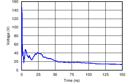
 Figure 11. +8-kV Contact ESD Clamping
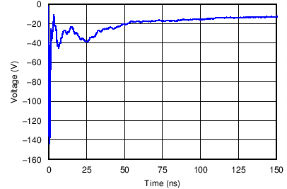
 Figure 12. –8-kV Contact ESD Clamping