SLVSDG5C March 2016 – August 2020 TPD3S014-Q1
PRODUCTION DATA
- 1 Features
- 2 Applications
- 3 Description
- 4 Revision History
- 5 Pin Configuration and Functions
-
6 Specifications
- 6.1 Absolute Maximum Ratings
- 6.2 ESD Ratings—AEC Specification
- 6.3 ESD Ratings—IEC Specification
- 6.4 ESD Ratings—ISO Specification
- 6.5 Recommended Operating Conditions
- 6.6 Thermal Information
- 6.7 Electrical Characteristics: TJ = TA = 25°C
- 6.8 Electrical Characteristics: –40°C ≤ TA ≤ 105°C
- 6.9 Typical Characteristics
- 7 Parameter Measurement Information
- 8 Detailed Description
- 9 Application and Implementation
- 10Power Supply Recommendations
- 11Layout
- 12Device and Documentation Support
- 13Mechanical, Packaging, and Orderable Information
Package Options
Mechanical Data (Package|Pins)
- DBV|6
Thermal pad, mechanical data (Package|Pins)
Orderable Information
8.3.2 Enable
The logic enable input (EN) controls the power switch, bias for the charge pump, driver, and other circuits. The supply current is reduced to less than 1 µA when the TPD3S014-Q1 is disabled. The enable input is compatible with both TTL and CMOS logic levels.
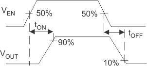
The turnon and turnoff times (tON, tOFF) are composed of a delay and a rise or fall time (tR, tF). The delay times are internally controlled. The rise time is controlled by both the TPD3S014-Q1 and the external loading (especially capacitance). The TPD3S014-Q1 fall time is controlled by the loading (R and C), and the output discharge (RPD). An output load consisting of only a resistor experiences a fall time set by the TPD3S014-Q1. An output load with parallel R and C elements experiences a fall time determined by the (R × C) time constant if it is longer than the TPD3S014-Q1 tF. See Figure 8-1 and Figure 8-2 showing tR, tF, tON, and tOFF. The enable must not be left open; it may be tied to VIN.
 Figure 8-1 Power-On and Power-Off Timing
 Figure 8-2 Enable Timing, Active-High Enable