SLVSCP4B October 2014 – August 2015 TPD3S014 , TPD3S044
PRODUCTION DATA.
- 1 Features
- 2 Applications
- 3 Description
- 4 Revision History
- 5 Device Comparison Table
- 6 Pin Configuration and Functions
- 7 Specifications
- 8 Detailed Description
- 9 Application and Implementation
- 10Power Supply Recommendations
- 11Layout
- 12Device and Documentation Support
- 13Mechanical, Packaging, and Orderable Information
Package Options
Mechanical Data (Package|Pins)
- DBV|6
Thermal pad, mechanical data (Package|Pins)
Orderable Information
9 Application and Implementation
NOTE
Information in the following applications sections is not part of the TI component specification, and TI does not warrant its accuracy or completeness. TI’s customers are responsible for determining suitability of components for their purposes. Customers should validate and test their design implementation to confirm system functionality.
9.1 Application Information
TPD3S0x4 are devices that feature a current limited load switch and a two-channel TVS based ESD protection diode array. They are typically used to provide a complete protection solution for USB host ports. USB host ports are required by the USB specification to provide a current limit on the VBUS path in order to protect the system from overcurrent conditions on the port that could lead to system damage and user injury. Additionally, USB ports typically require system level IEC ESD protection due to direct end-user interaction. The following design procedure can be used to determine how to properly implement TPD3S0x4s in your systems to provide a complete, one-chip solution for your USB ports.
9.2 Typical Applications
9.2.1 USB2.0 Application
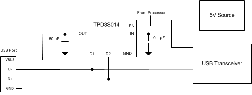 Figure 30. USB2.0 Application Schematic
9.2.1.1 Design Requirements
For this design example, use the following as the system parameters.
Table 1. Design Parameters
| DESIGN PARAMETER | VALUE |
|---|---|
| USB port type | Standard downstream port |
| Signal voltage range on VBUS | 0 V to 5.25 V |
| Current range on VBUS | 0 mA to 500 mA |
| Drive EN low (disabled) | 0 V to 0.7 V(1) |
| Drive EN high (enabled) | 2 V to 5.5 V(1) |
| Maximum voltage droop allowed on adjacent USB port | 330 mV |
| Maximum data rate | 480 Mbps |
9.2.1.2 Detailed Design Procedure
To properly implement your USB port with TPD3S0x4s, the first step is to determine what type of USB port you are implementing in your system, whether it be a Standard Downstream Port (SDP), Charging Downstream Port (CDP), or Dedicated Charging Port (DCP); this will inform you what your maximum continuous operating current will be on VBUS. In our example, we are implementing an SDP port, so the maximum continuous current allowed to be pulled by a device is 500mA. Therefore, we need to choose a current limit switch that is 5.25V tolerant, can handle 500mA continuous DC current, and has a current limit point is above 500 mA so it will not current limit during normal operation. TPD3S014 is therefore the best choice for this application, as it has these features, and in fact was specifically designed for this application.
The next decision point is choosing your input and output capacitors for your current limit switch. A minimum of 0.1 µF is always recommended on the IN pin. For the OUT pin on VBUS, USB standard requires a minimum of 120 µF; typically a 150 µF capacitor is used. The purpose of the capacitance requirement on the VBUS line in the USB specification is to prevent the adjacent USB port's VBUS voltage from dropping more than 330 mV during a hot-plug or fault occurrence on the VBUS pin of one USB port. Hot-plugs and fault conditions on one USB port should not disturb the normal operation of an adjacent USB port; therefore, it is possible to use an output capacitance lower than 120 µF if your system is able to keep voltage droops on adjacent USB ports less than or equal to 330 mV. For example, if the DC/DC powering VBUS has a fast transient response, 120 µF may not be required.
If your USB port is powered from a shared system 5V rail, a system designer may desire to use an input capacitor larger than 0.1 µF on the IN pin. This is largely dependent on your PCB layout and parasitics, as well as your maximum tolerated voltage droop on the shared rail during transients. For more information on choosing input and output capacitors, see Input and Output Capacitance.
The EN pin controls the on and off state of the device, and typically is connected to the system processor for power sequencing. However, the EN pin can also be shorted to the IN pin to always have the TPD3S014 on when 5-V power supply on; this also saves a GPIO pin on your processor.
For a USB port with High-Speed 480Mbps operation, low capacitance TVS ESD protection diodes are required to protect the D+ and D- lines in the event of system level ESD event. TPD3S014 has 2-channels of low capacitance TVS ESD protection diodes integrated. When placed near the USB connector, TPD3S014 offers little or no signal distortion during normal operation. TPD3S014 also ensures that the core system circuitry is protected in the event of an ESD strike. PCB layout is critical when implementing TVS ESD protection diodes in your system; please read the Layout section for proper guidelines on routing your USB lines with TPD3S014.
9.2.1.3 Implementing Active Low Logic
For active low logic, a transistor can be used with the TPD3S014 EN Pin.
|
Using an nFET transistor, when the Processor sends a low signal, the transistor is switched off, and VLOGIC pulls up EN through R1. When the Processor sends a “high” signal, the nFET is switched on and sinks current from the EN Pin and R1. For 5-V VLOGIC, with the appropriate on-resistance (RON) value in the nFET and resistance for R1, the VIL for EN can be met. For example, with a transistor with RON of 3-Ω, a pull-up resistor as low as 11 Ω provides a logic level of 0.7 V. For power-budgeting concerns, a better choice is R1 of 40-kΩ which provides 0.25 V for EN when the Processor asserts high, and 4.96 V when the Processor asserts low. |
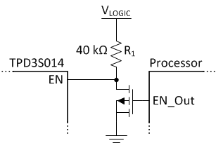 Figure 31. Implementing Active Low Logic for EN Pin Figure 31. Implementing Active Low Logic for EN Pin
|
|
9.2.1.4 Application Curves
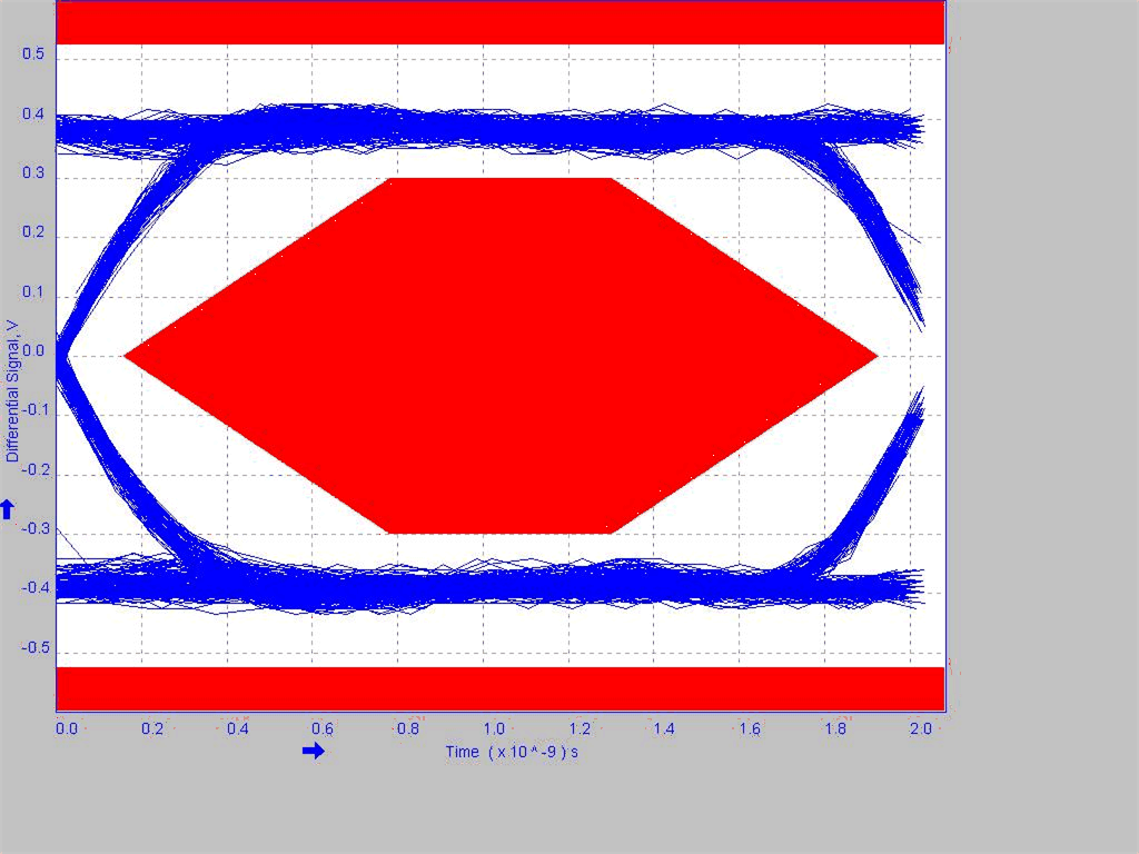 Figure 32. Eye-Diagram Without EVM
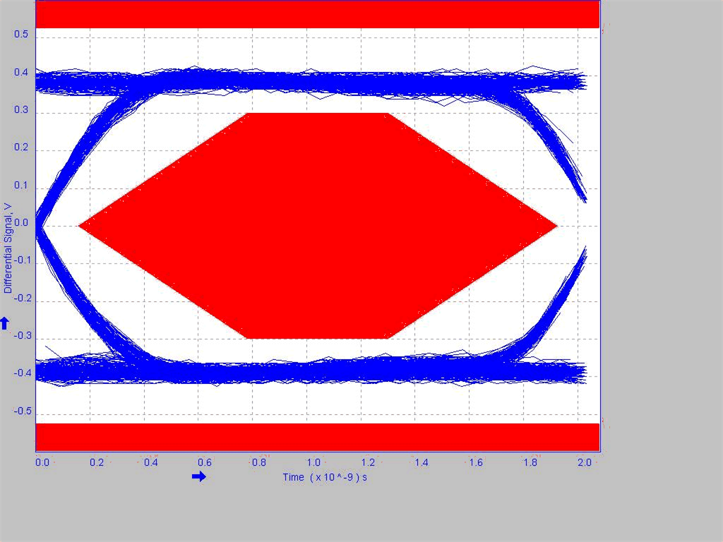 Figure 34. Eye-Diagram of TPD3S0x4 on EVM
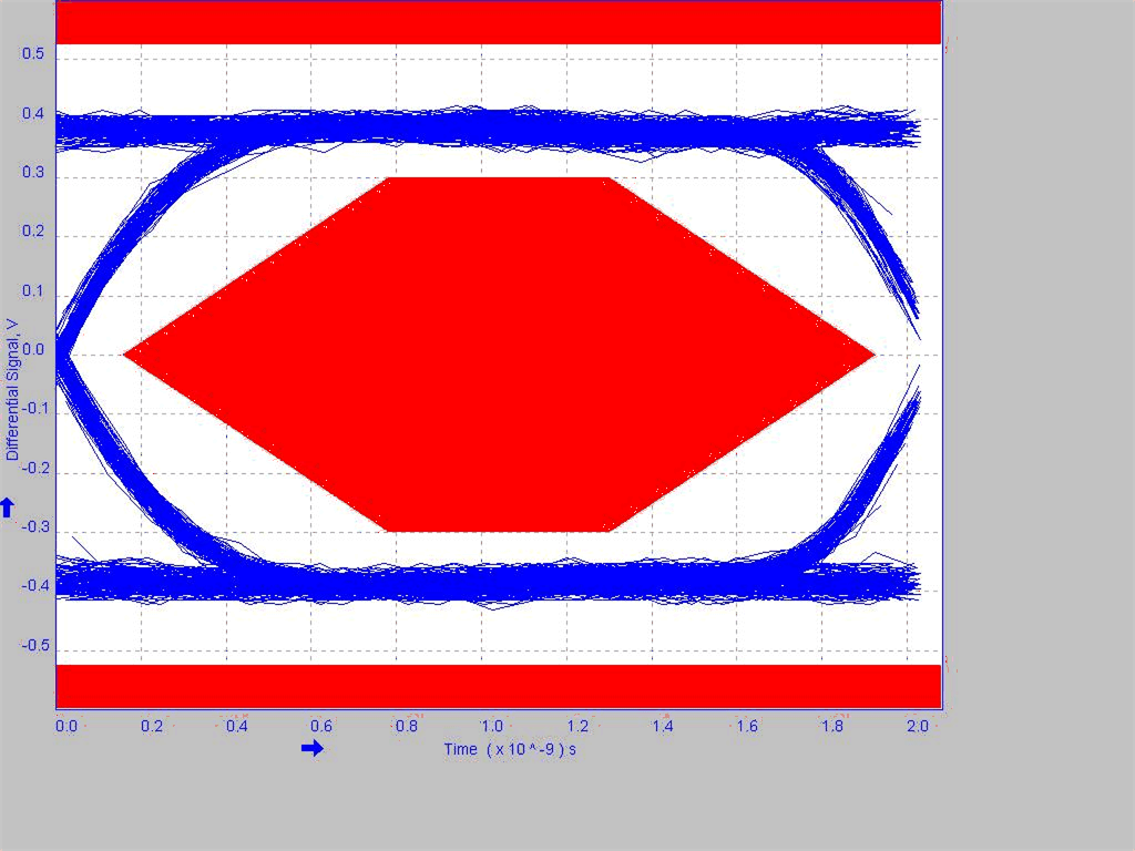 Figure 33. Eye-Diagram With EVM, Without TPD3S0x4
9.2.2 USB3.0 Application
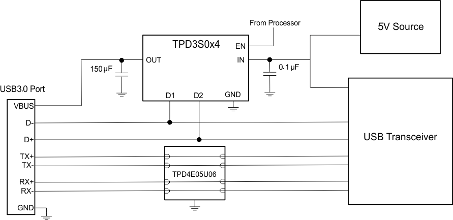 Figure 35. USB3.0 Application Schematic
9.2.2.1 Design Requirements
For this design example, use the following as the system parameters.
Table 2. Design Parameters
| DESIGN PARAMETER | VALUE |
|---|---|
| USB port type | Standard downstream port |
| Signal voltage range on VBUS | 0 V to 5.25 V |
| Current range on VBUS | 0 mA to 900 mA |
| Maximum voltage droop allowed on adjacent USB port | 330 mV |
| Maximum data rate D+, D- lines | 480 Mbps |
| Maximum data rate TX±, RX± lines | 5 Gbps |
9.2.2.2 Detailed Design Procedure
The implementation of the USB3.0 port with TPD3S0x4s is identical to the USB2.0 port, except that in this use case we must use TPD3S044 because USB3.0 SDP has a maximum VBUS current 900 mA. TPD3S014 current limit level is too low for USB3.0 operation. In addition to using TPD3S044, USB3.0 has four more Super-Speed Lines for transferring data 5 Gbps, and these lines also typically require Level 4 IEC61000-4-2 ESD Protection. With a data rate of 5 Gbps, ultra-low capacitance TVS ESD protection diodes are required to protect the TX± and RX± lines in the event of system level ESD event. TPD4E05U06 provides 4-channels of ultra-low capacitance TVS ESD protection diodes for USB3.0 Super-Speed lines, and can be coupled with TPD3S044 to provide a two-chip total protection solution for the USB3.0 host port. Please refer to the Layout section of the data sheet for guidelines on the PCB layout of this two-chip solution.
The rest of the design procedure is identical to the USB2.0 Application section, so refer to it for the rest of the design procedure.
9.2.2.3 Application Curves
See Application Curves for TPD3S0x4 eye-diagram performance. Refer to the TPD4E05U06 data sheet on ti.com to see its specifications and eye-diagram performance.