SLVSCP4B October 2014 – August 2015 TPD3S014 , TPD3S044
PRODUCTION DATA.
- 1 Features
- 2 Applications
- 3 Description
- 4 Revision History
- 5 Device Comparison Table
- 6 Pin Configuration and Functions
- 7 Specifications
- 8 Detailed Description
- 9 Application and Implementation
- 10Power Supply Recommendations
- 11Layout
- 12Device and Documentation Support
- 13Mechanical, Packaging, and Orderable Information
Package Options
Mechanical Data (Package|Pins)
- DBV|6
Thermal pad, mechanical data (Package|Pins)
Orderable Information
8 Detailed Description
8.1 Overview
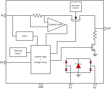
The TPD3S0x4 are highly integrated devices that feature a current limited load switch and a two-channel TVS based ESD protection diode array for USB interfaces. The TPD3S014 and TPD3S044 provide 0.5 A and 1.5 A, respectively, of continuous load current in 5-V circuits. These parts use N-channel MOSFETs for low resistance, maintaining voltage regulation to the load. It is designed for applications where short circuits or heavy capacitive loads will be encountered. Device features include enable, reverse blocking when disabled, output discharge pull-down, overcurrent protection, and overtemperature protection. Finally, with two channels of TVS ESD protection diodes integrated, TPD3S0x4s provide system level ESD protection to all the pins of the USB port.
8.2 Functional Block Diagram
8.3 Feature Description
8.3.1 Undervoltage Lockout (UVLO)
The UVLO circuit disables the power switch until the input voltage reaches the UVLO turn-on threshold. Built-in hysteresis prevents unwanted on/off cycling due to input voltage drop from large current surges.
8.3.2 Enable
The logic enable input (EN) controls the power switch, bias for the charge pump, driver, and other circuits. The supply current is reduced to less than 1 µA when the TPD3S0x4s are disabled. The enable input is compatible with both TTL and CMOS logic levels.
The turn on and turn off times (tON, tOFF) are composed of a delay and a rise or fall time (tR, tF). The delay times are internally controlled. The rise time is controlled by both the TPD3S0x4s and the external loading (especially capacitance). TPD3S0x4s fall time is controlled by the loading (R and C), and the output discharge (RPD). An output load consisting of only a resistor will experience a fall time set by the TPD3S0x4s. An output load with parallel R and C elements will experience a fall time determined by the (R × C) time constant if it is longer than the TPD3S0x4’s tF. See Figure 25 and Figure 26 for a pictural description of tR, tF, tON, and tOFF. The enable should not be left open; it may be tied to VIN.
 Figure 25. Power-On and Power-Off Timing
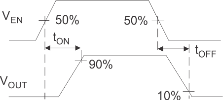 Figure 26. Enable Timing, Active-High Enable
8.3.3 Internal Charge Pump
The device incorporates an internal charge pump and gate drive circuitry necessary to drive the N-channel MOSFET. The charge pump supplies power to the gate driver circuit and provides the necessary voltage to pull the gate of the MOSFET above the source. The driver incorporates circuitry that controls the rise and fall times of the output voltage to limit large current and voltage surges on the input supply, and provides built-in soft-start functionality. The MOSFET power switch will block current from OUT to IN when turned off by the UVLO or disabled.
8.3.4 Current Limit
The TPD3S0x4s respond to overloads by limiting output current to the static current-limit (IOS) levels shown in the Electrical Characteristics: TJ = TA = 25°C table. When an overload condition is present, the device maintains a constant output current, with the output voltage determined by (IOS × RLOAD). Two possible overload conditions can occur.
The first overload condition occurs when either:
- The input voltage is first applied, enable is true, and a short circuit is present (load which draws IOUT > IOS) or
- The input voltage is present and the TPD3S0x4s are enabled into a short circuit.
The output voltage is held near zero potential with respect to ground and the TPD3S0x4s ramp the output current to IOS. The TPD3S0x4s will limit the current to IOS until the overload condition is removed or the device begins to thermal cycle. The device subsequently cycles current off and on as the thermal protection engages.
The second condition is when an overload occurs while the device is enabled and fully turned on. The device responds to the overload condition within tIOS (Figure 27 and Figure 28) when the specified overload (per Electrical Characteristics table) is applied. The response speed and shape will vary with the overload level, input circuit, and rate of application. The current-limit response will vary between simply settling to IOS, or turnoff and controlled return to IOS. Similar to the previous case, the TPD3S0x4s will limit the current to IOS until the overload condition is removed or the device begins to thermal cycle.
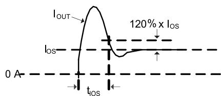 Figure 27. Output Short Circuit Parameters
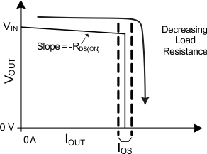 Figure 28. Output Characteristic Showing Current Limit
The TPD3S0x4s thermal cycle if an overload condition is present long enough to activate thermal limiting in any of the above cases. This is due to the relatively large power dissipation [(VIN – VOUT) × IOS] driving the junction temperature up. The devices turn off when the junction temperature exceeds 135°C (min) while in current limit. The devices remains off until the junction temperature cools 20°C and then restarts.
There are two kinds of current limit profiles typically available in TI switch products similar to the TPD3S0x4s. Many older designs have an output I vs V characteristic similar to the plot labeled "Current Limit with Peaking" in Figure 29. This type of limiting can be characterized by two parameters, the current limit corner (IOC), and the short circuit current (IOS). IOC is often specified as a maximum value. The TPD3S0x4 parts do not present noticeable peaking in the current limit, corresponding to the characteristic labeled "Flat Current Limit" in Figure 29. This is why the IOC parameter is not present in the Electrical Characteristics tables.
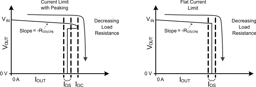 Figure 29. Current Limit Profiles
8.3.5 Output Discharge
A 470-Ω (typical) output discharge resistance will dissipate stored charge and leakage current on OUT when the TPD3S0x4s are in UVLO or disabled. The pull-down circuit will lose bias gradually as VIN decreases, causing a rise in the discharge resistance as VIN falls towards 0 V.
8.3.6 Input and Output Capacitance
Input and output capacitance improves the performance of the device; the actual capacitance should be optimized for the particular application. For all applications, a 0.1 µF or greater ceramic bypass capacitor between IN and GND is recommended as close to the device as possible for local noise decoupling.
All protection circuits such as the TPD3S0x4s will have the potential for input voltage overshoots and output voltage undershoots.
Input voltage overshoots can be caused by either of two effects. The first cause is an abrupt application of input voltage in conjunction with input power bus inductance and input capacitance when the IN terminal is high impedance (before turn on). Theoretically, the peak voltage is 2 times the applied. The second cause is due to the abrupt reduction of output short circuit current when the TPD3S0x4s turn off and energy stored in the input inductance drives the input voltage high. Input voltage droops may also occur with large load steps and as the TPD3S0x4s outputs are shorted. Applications with large input inductance (for example, connecting the evaluation board to the bench power-supply through long cables) may require large input capacitance reduce the voltage overshoot from exceeding the absolute maximum voltage of the device. The fast current-limit speed of the TPD3S0x4s to hard output short circuits isolates the input bus from faults. However, ceramic input capacitance in the range of 1 to 22 µF adjacent to the TPD3S0x4s inputs aids in both speeding the response time and limiting the transient seen on the input power bus. Momentary input transients to 6.5 V are permitted.
Output voltage undershoot is caused by the inductance of the output power bus just after a short has occurred and the TPD3S0x4s have abruptly reduced OUT current. Energy stored in the inductance will drive the OUT voltage down and potentially negative as it discharges. Applications with large output inductance (such as from a cable) benefit from use of a high-value output capacitor to control the voltage undershoot. When implementing USB standard applications, a 120 µF minimum output capacitance is required. Typically a 150-µF electrolytic capacitor is used, which is sufficient to control voltage undershoots. However, if the application does not require 120 µF of capacitance, and there is potential to drive the output negative, a minimum of 10-µF ceramic capacitance on the output is recommended. The voltage undershoot should be controlled to less than 1.5 V for 10 µs.
8.4 Device Functional Modes
8.4.1 Operation With VIN < 4 V (Minimum VIN)
These devices operate with input voltages above 4 V. The maximum UVLO voltage on IN is 4 V and the devices will operate at input voltages above 4 V. Any voltage below 4 V may not work with these devices. The minimum UVLO is 3.5 V, so some devices may work between 3.5 V and 4 V. At input voltages below the actual UVLO voltage, these devices will not operate.
8.4.2 Operation With EN Control
The enable rising edge threshold voltage is 1.45 V typical and 2 V maximum. With EN held below that voltage the device is disabled and the load switch will be open. The IC quiescent current is reduced in this state. When the EN pin is above its rising edge threshold and the input voltage on the IN pin is above its UVLO threshold, the device becomes active. The load switch is closed, and the current limit feature is enabled. The output voltage on OUT will ramp up with the soft start value TON in order to prevent large inrush current surges on VBUS due to a heavy capacitive load. When EN voltage is lowered below is falling edge threshold, the device output voltage will also ramp down with soft turn off value TOFF to prevent large inductive voltages being presented to the system in the case a large load current is following through the device.
8.4.3 Operation of Level 4 IEC61000-4-2 ESD Protection
Regardless of which functional mode the devices are in, TPD3S0x4 will provide Level 4 IEC61000-4-2 ESD Protection on the pins of the USB connector.