SLLSEG0F March 2013 – September 2017 TPD4E001-Q1
PRODUCTION DATA.
- 1 Features
- 2 Applications
- 3 Description
- 4 Revision History
- 5 Pin Configuration and Functions
- 6 Specifications
- 7 Detailed Description
- 8 Application and Implementation
- 9 Power Supply Recommendations
- 10Layout
- 11Device and Documentation Support
- 12Mechanical, Packaging, and Orderable Information
Package Options
Mechanical Data (Package|Pins)
- DBV|6
Thermal pad, mechanical data (Package|Pins)
Orderable Information
8 Application and Implementation
NOTE
Information in the following applications sections is not part of the TI component specification, and TI does not warrant its accuracy or completeness. TI’s customers are responsible for determining suitability of components for their purposes. Customers should validate and test their design implementation to confirm system functionality.
8.1 Application Information
The TPD4E001-Q1 device is a TVS diode array which is typically used to provide a path to ground for dissipating ESD events on high-speed signal lines between a human interface connector and a system. As the current from ESD passes through the TVS, only a small voltage drop is present across the diode. This is the voltage presented to the protected IC. The triggered TVS holds this voltage, VCLAMP, to a safe level for the protected IC.
8.2 Typical Application
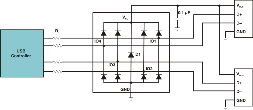
For this design example, one TPD4E001-Q1 device is being used in a dual USB 2.0 application. This provides a complete port protection scheme.
8.2.1 Design Requirements
For this design example, a single TPD4E001-Q1 device is used to protect all the pins on two USB2.0 connectors.
Given the USB application, known parameters are listed in the Table 1.
Table 1. Design Parameters
| DESIGN PARAMETER | VALUE |
|---|---|
| Signal range on IO1, IO2, IO3, or IO4 | 0 V to 3.6 V |
| Voltage range on VCC | 0 V to 5.25 V |
| Operating Frequency on IO1, IO2, IO3, or IO4 | 240 MHz |
8.2.2 Detailed Design Procedure
To begin the design process, some parameters must be decided upon; the designer needs to know the following:
- Signal range on all protected lines
- Operating frequency on all protected lines
8.2.2.1 Signal Range on IO1 Through IO4
The TPD4E001-Q1 device has 4 identical protection channels for signal lines. The symmetry of the device provides flexibility when selecting which of the 4 IO channels protects which signal lines. Any IO supports a signal range of 0 to (VCC + 0.3) V. Therefore, this device supports the USB 2.0 signal swing assuming VCC is set appropriately.
8.2.2.2 Voltage Range on VCC
The VCC pin can be connected in one of two ways:
- If the VCC pin connects to the system power supply, the TPD4E001-Q1 device works as a transient suppressor for any signal swing above VCC + VF. TI recommends a 0.1-μF capacitor on the device VCC pin for ESD bypass.
- If the VCC pin does not connect to the system power supply, the TPD4E001-Q1 device can tolerate higher signal swing in the range up to 10 V. Note that TI still recommends a 0.1-μF capacitor at the VCC pin for ESD bypass.
If this pin is connected to the USB 2.0 VBUS supply or left floating, the allowable signal swing is enough for a USB 2.0 application.
8.2.2.3 Bandwidth on IO1 Through IO4
Each IO pin on the TPD4E001-Q1 device has a typical capacitance of 1.5 pF. This capacitance is low enough to easily support USB 2.0 data rates.
8.2.3 Application Curve
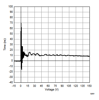
 Figure 5. IEC 61000-4-2 Voltage Clamp Waveform 8-kV Contact
