SLVSDZ2A June 2017 – September 2017 TPD4E02B04-Q1
PRODUCTION DATA.
- 1 Features
- 2 Applications
- 3 Description
- 4 Revision History
- 5 Pin Configuration and Functions
- 6 Specifications
-
7 Detailed Description
- 7.1 Overview
- 7.2 Functional Block Diagram
- 7.3
Feature Description
- 7.3.1 AEC-Q101 Qualified
- 7.3.2 ISO 10605 ESD Protection
- 7.3.3 IEC 61000-4-2 ESD Protection
- 7.3.4 IEC 61000-4-4 EFT Protection
- 7.3.5 IEC 61000-4-5 Surge Protection
- 7.3.6 IO Capacitance
- 7.3.7 DC Breakdown Voltage
- 7.3.8 Ultra Low Leakage Current
- 7.3.9 Low ESD Clamping Voltage
- 7.3.10 Supports High Speed Interfaces
- 7.3.11 Industrial Temperature Range
- 7.3.12 Easy Flow-Through Routing Package
- 7.4 Device Functional Modes
- 8 Application and Implementation
- 9 Power Supply Recommendations
- 10Layout
- 11Device and Documentation Support
- 12Mechanical, Packaging, and Orderable Information
Package Options
Mechanical Data (Package|Pins)
- DQA|10
Thermal pad, mechanical data (Package|Pins)
- DQA|10
Orderable Information
6 Specifications
6.1 Absolute Maximum Ratings
over operating free-air temperature range (unless otherwise noted)(1)| MIN | MAX | UNIT | ||
|---|---|---|---|---|
| Electrical fast transient | IEC 61000-4-5 (5/50 ns) at 25°C | 80 | A | |
| Peak pulse | IEC 61000-4-5 power (tp - 8/20 µs) at 25°C | 17 | W | |
| IEC 61000-4-5 Ccurrent (tp - 8/20 µs) at 25°C | 2 | A | ||
| TA | Operating free-air temperature | –40 | 125 | °C |
| Tstg | Storage temperature | –65 | 155 | °C |
(1) Stresses beyond those listed under Absolute Maximum Ratings may cause permanent damage to the device. These are stress ratings only, which do not imply functional operation of the device at these or any other conditions beyond those indicated under Recommended Operating Conditions. Exposure to absolute-maximum-rated conditions for extended periods may affect device reliability.
6.2 ESD Ratings—AEC Specification
| VALUE | UNIT | |||
|---|---|---|---|---|
| V(ESD) | Electrostatic discharge | Human-body model (HBM), per AEC Q100-002(1) | ±2500 | V |
| Charged-device model (CDM), per AEC Q100-011 | ±1000 | |||
(1) AEC Q100-002 indicates that HBM stressing shall be in accordance with the ANSI/ESDA/JEDEC JS-001 specification.
6.3 ESD Ratings—IEC Specification
| VALUE | UNIT | |||
|---|---|---|---|---|
| V(ESD) | Electrostatic discharge | IEC 61000-4-2 contact discharge | ±12000 | V |
| IEC 61000-4-2 air-gap discharge | ±15000 | |||
6.4 ESD Ratings—ISO Specification
| VALUE | UNIT | ||||
|---|---|---|---|---|---|
| V(ESD) | Electrostatic discharge | ISO 10605 330 pF, 330 Ω, IO | Contact discharge | ±10000 | V |
| Air-gap discharge | ±10000 | ||||
6.5 Recommended Operating Conditions
over operating free-air temperature range (unless otherwise noted)| MIN | MAX | UNIT | ||
|---|---|---|---|---|
| VIO | Input pin voltage | –3.6 | 3.6 | V |
| TA | Operating free-air temperature | –40 | 125 | °C |
6.6 Thermal Information
| THERMAL METRIC(1) | TPD4E02B04-Q1 | UNIT | |
|---|---|---|---|
| DQA (USON) | |||
| 10 PINS | |||
| RθJA | Junction-to-ambient thermal resistance | 348.7 | °C/W |
| RθJC(top) | Junction-to-case (top) thermal resistance | 214.1 | °C/W |
| RθJB | Junction-to-board thermal resistance | 270.7 | °C/W |
| ψJT | Junction-to-top characterization parameter | 81.7 | °C/W |
| ψJB | Junction-to-board characterization parameter | 270.7 | °C/W |
| RθJC(bot) | Junction-to-case (bottom) thermal resistance | N/A | °C/W |
(1) For more information about traditional and new thermal metrics, see the Semiconductor and IC Package Thermal Metrics application report.
6.7 Electrical Characteristics
over operating free-air temperature range (unless otherwise noted)| PARAMETER | TEST CONDITIONS | MIN | TYP | MAX | UNIT | |
|---|---|---|---|---|---|---|
| VRWM | Reverse stand-off voltage | IIO < 10 nA | –3.6 | 3.6 | V | |
| VBRF | Breakdown voltage, any IO pin to GND(1) | IIO = 1 mA, TA = 25°C | 5.5 | 6.4 | 7.5 | V |
| VBRR | Breakdown voltage, GND to any IO pin(1) | IIO = 1 mA, TA = 25°C | –5.5 | –6.4 | –7.5 | V |
| VHOLD | Holding voltage(2) | IIO = 1 mA | 5.8 | V | ||
| VCLAMP | Clamping voltage | IPP = 1 A, TLP, from IO to GND | 6.6 | V | ||
| IPP = 5 A, TLP, from IO to GND | 8.8 | |||||
| IPP = 1 A, TLP, from GND to IO | 6.6 | |||||
| IPP = 5 A, TLP, from GND to IO | 8.8 | |||||
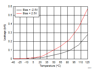
| ILEAK | Leakage current, any IO to GND | VIO = ±2.5 V | 10 | nA | ||
| RDYN | Dynamic resistance | IO to GND | 0.47 | Ω | ||
| GND to IO | 0.47 | |||||
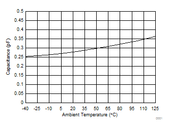
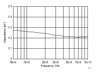
| CL | Line capacitance | VIO = 0 V, f = 1 MHz, IO to GND, TA = 25°C | 0.25 | 0.33 | pF | |
| ΔCL | Variation of line capacitance | Delta of capacitance between any two IO pins, VIO = 0 V, f = 1 MHz, TA = 25°C, GND = 0 V | 0.01 | 0.07 | pF | |
| CCROSS | Channel to channel capacitance | Capacitance from one IO to another, VIO = 0 V, f = 1 MHz, GND = 0 V | 0.13 | 0.16 | pF | |
(1) VBRF and VBRR are defined as the voltage when 1 mA is applied in the positive-going direction, before the device latches into the snapback state.
(2) VHOLD is defined as the voltage when 1 mA is applied in the negative-going direction, after the device has successfully latched into the snapback state.
6.8 Typical Characteristics


(With TPD4E02B04-Q1)
