SLVSBO7O December   2012  – August 2024 TPD1E05U06 , TPD4E05U06 , TPD6E05U06

PRODUCTION DATA  

  1.   1
  2. Features
  3. Applications
  4. Description
  5. Pin Configuration and Functions
  6. Specifications
    1.     Absolute Maximum Ratings
    2. 5.1 ESD Ratings—JEDEC Specification
    3. 5.2 ESD Ratings—IEC Specification
    4.     Recommended Operating Conditions
    5. 5.3 Thermal Information
    6. 5.4 Electrical Characteristics
    7. 5.5 Typical Characteristics
  7. Detailed Description
    1. 6.1 Overview
    2. 6.2 Functional Block Diagram
    3. 6.3 Feature Description
      1. 6.3.1 ±15-kV IEC61000-4-2 Level 4 ESD Protection
      2. 6.3.2 IEC61000-4-4 EFT Protection
      3. 6.3.3 IEC61000-4-5 Surge Protection
      4. 6.3.4 I/O Capacitance
      5. 6.3.5 DC Breakdown Voltage
      6. 6.3.6 Ultra-Low Leakage Current
      7. 6.3.7 Low ESD Clamping Voltage
      8. 6.3.8 Industrial Temperature Range
      9. 6.3.9 Easy Flow-Through Routing
    4. 6.4 Device Functional Modes
  8. Application and Implementation
    1. 7.1 Application Information
    2. 7.2 Typical Applications
      1. 7.2.1 HDMI 2.0 Application
        1. 7.2.1.1 Design Requirements
        2. 7.2.1.2 Detailed Design Procedure
          1. 7.2.1.2.1 Signal Range on Pin 1, 2, 4, or 5
        3. 7.2.1.3 Application Curves
      2. 7.2.2 HDMI 2.0 Application
        1. 7.2.2.1 Design Requirements
        2. 7.2.2.2 Detailed Design Procedure
          1. 7.2.2.2.1 Signal Range
          2. 7.2.2.2.2 Operating Frequency
        3. 7.2.2.3 Application Curves
    3. 7.3 Power Supply Recommendations
    4. 7.4 Layout
      1. 7.4.1 Layout Guidelines
      2. 7.4.2 Layout Example
        1. 7.4.2.1 TPD4E05U06 Layout Example
        2. 7.4.2.2 TPD1E05U06 Layout Example
  9. Device and Documentation Support
    1. 8.1 Documentation Support
      1. 8.1.1 Related Documentation
    2. 8.2 Receiving Notification of Documentation Updates
    3. 8.3 Support Resources
    4. 8.4 Trademarks
    5. 8.5 Electrostatic Discharge Caution
    6. 8.6 Glossary
  10. Revision History
  11. 10Mechanical, Packaging, and Orderable Information
    1. 10.1 Tape and Reel Information
    2. 10.2 Mechanical Data

Package Options

Refer to the PDF data sheet for device specific package drawings

Mechanical Data (Package|Pins)
  • DQA|10
Thermal pad, mechanical data (Package|Pins)
Orderable Information

Description

The TPDxE05U06 is a family of unidirectional Transient Voltage Suppressor (TVS) based Electrostatic Discharge (ESD) protection diodes with ultra-low capacitance. Each device can dissipate ESD strikes above the maximum level specified by the IEC 61000-4-2 international standard. The TPDxE05U06 ultra-low loading capacitance makes the device and excellent choice for protecting any high-speed signal pins.

Typical applications for TPDxE05U06 includes high speed signal lines in HDMI 1.4b, HDMI 2.0, USB 3.0, MHL, LVDS, DisplayPort, PCI-Express®, eSata, and V-by-One® HS.

Device Information
PART NUMBER CHANNEL COUNT PACKAGE(1)
TPD1E05U06 1 channel DPY (X1SON, 2)
DYA (SOD-523, 2)
TPD4E05U06 4 channels DQA (USON, 10)
TPD6E05U06 6 channels RVZ (USON, 14)
For more information, see Section 10.
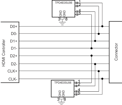
TPD1E05U06 TPD4E05U06 TPD6E05U06 Simplified SchematicSimplified Schematic
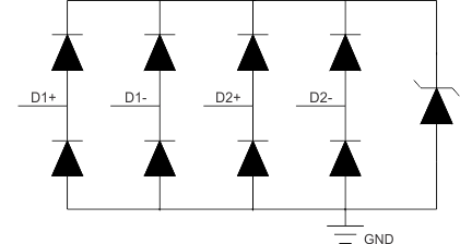
TPD1E05U06 TPD4E05U06 TPD6E05U06 TPD4E05U06 Functional Block
                        DiagramTPD4E05U06 Functional Block Diagram