SLVSBQ9D December 2012 – April 2017 TPD4E1U06
PRODUCTION DATA.
- 1 Features
- 2 Applications
- 3 Description
- 4 Revision History
- 5 Pin Configuration and Functions
- 6 Specifications
- 7 Detailed Description
- 8 Application and Implementation
- 9 Power Supply Recommendations
- 10Layout
- 11Device and Documentation Support
- 12Mechanical, Packaging, and Orderable Information
Package Options
Mechanical Data (Package|Pins)
Thermal pad, mechanical data (Package|Pins)
Orderable Information
6 Specifications
6.1 Absolute Maximum Ratings
over operating free-air temperature range (unless otherwise noted) (1)
(1) Stresses beyond those listed under Absolute Maximum Ratings may cause permanent damage to the device. These are stress ratings only, which do not imply functional operation of the device at these or any other conditions beyond those indicated under Recommended Operating Conditions. Exposure to absolute-maximum-rated conditions for extended periods may affect device reliability.
6.2 ESD Ratings
| VALUE | UNIT | |||
|---|---|---|---|---|
| V(ESD) | Electrostatic discharge | Human body model (HBM), per ANSI/ESDA/JEDEC JS-001, all pins(1) | ±4000 | V |
| Charged device model (CDM), per JEDEC specification JESD22-C101, all pins(2) | ±1500 | |||
(1) JEDEC document JEP155 states that 500-V HBM allows safe manufacturing with a standard ESD control process.
(2) JEDEC document JEP157 states that 250-V CDM allows safe manufacturing with a standard ESD control process.
6.3 ESD Ratings—IEC Specification
| VALUE | UNIT | |||
|---|---|---|---|---|
| V(ESD) | Electrostatic discharge | IEC 61000-4-2 contact ESD | ±15000 | V |
| IEC 61000-4-2 air-gap ESD | ±15000 | |||
6.4 Recommended Operating Conditions
over operating free-air temperature range (unless otherwise noted)| MIN | MAX | UNIT | ||
|---|---|---|---|---|
| VIO | Input pin voltage | 0 | 5.5 | V |
| TA | Operating free-air temperature | –40 | 125 | °C |
6.5 Thermal Information
| THERMAL METRIC(1) | TPD4E1U06 | UNIT | ||
|---|---|---|---|---|
| DBV (SOT-23) | DCK (SC-70) | |||
| 6 PINS | 6 PINS | |||
| RθJA | Junction-to-ambient thermal resistance | 224.3 | 274.3 | °C/W |
| RθJC(top) | Junction-to-case (top) thermal resistance | 166.1 | 113.8 | °C/W |
| RθJB | Junction-to-board thermal resistance | 68.4 | 76.7 | °C/W |
| ψJT | Junction-to-top characterization parameter | 57.3 | 3.6 | °C/W |
| ψJB | Junction-to-board characterization parameter | 67.9 | 75.9 | °C/W |
(1) For more information about traditional and new thermal metrics, see the Semiconductor and IC Package Thermal Metrics application report.
6.6 Electrical Characteristics
over recommended operating free-air temperature range (unless otherwise noted)| PARAMETER | TEST CONDITIONS | MIN | TYP | MAX | UNIT | ||
|---|---|---|---|---|---|---|---|
| VRWM | Reverse stand-off voltage | IIO = 10 µA | 5.5 | V | |||
| VCLAMP | Clamp voltage with ESD strike | IPP = 1 A, tp = 8/20 μs, from I/O to GND(1) | 11 | V | |||
| IPP = 3 A, tp = 8/20 μs, from I/O to GND(1) | 15 | V | |||||
| RDYN | Dynamic resistance | Pin x to GND pin(2) | 1.0 | Ω | |||
| GND to pin x | 0.6 | ||||||
| CL | Line capacitance | f = 1 MHz, VBIAS = 2.5 V, 25°C | 0.8 | 1 | pF | ||
| CCROSS | Channel to channel input capacitance | Pin 2 = 0 V, f = 1 MHz, VBIAS = 2.5 V, between channel pins | DCK package | 0.006 | 0.015 | pF | |
| DBV package | 0.01 | 0.025 | |||||
| ∆CIO-TO-GND | Variation of channel input capacitance | Pin 2 = 0 V , f = 1 MHz, VBIAS = 2.5 V, channel_x pin to ground – channel_y pin to ground | 0.025 | 0.07 | pF | ||
| VBR | Break-down voltage, IO to GND | IIO = 1 mA | 6.5 | 8.5 | V | ||
| ILEAK | Leakage current | VIO = 2.5 V | 1 | 10 | nA | ||
(1) Non-repetitive current pulse 8/20 µs exponentially decaying waveform according to IEC61000-4-5.
(2) Extraction of RDYN using least squares fit of TLP characteristics between I = 10 A and I = 20 A.
6.7 Typical Characteristics
 Figure 1. TLP, Data to GND
 Figure 3. IEC 61000-4-2 Clamping Voltage, 8-kV Contact
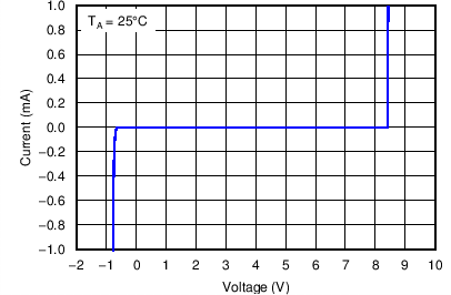
 Figure 5. Diode Curve
 Figure 7. Capacitance Across VBIAS
 Figure 2. TLP, GND to Data
 Figure 4. IEC 61000-4-2 Clamping Voltage, –8-kV Contact
 Figure 6. ILEAK vs Temperature
 Figure 8. Surge Curve (tp = 8/20 μs), Pin IO to GND