-
TPD4E6B06 4-Channel Bidirectional Low Capacitance ESD Protection Device With 15-kV Contact and Ultra-Low Clamping Voltage
- 1 Features
- 2 Applications
- 3 Description
- 4 Revision History
- 5 Pin Configuration and Functions
- 6 Specifications
- 7 Detailed Description
- 8 Application and Implementation
- 9 Power Supply Recommendations
- 10Layout
- 11Device and Documentation Support
- 12Mechanical, Packaging, and Orderable Information
- IMPORTANT NOTICE
Package Options
Mechanical Data (Package|Pins)
- DPW|4
Thermal pad, mechanical data (Package|Pins)
- DPW|4
Orderable Information
TPD4E6B06 4-Channel Bidirectional Low Capacitance ESD Protection Device With 15-kV Contact and Ultra-Low Clamping Voltage
1 Features
- IEC 61000-4-2 Level 4
- ±15-kV Contact Discharge
- ±15-kV Air Gap Discharge
- IEC 61000-4-5 (Surge): 3 A (8/20 µs)
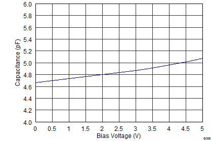
- IO Capacitance: 4.8 pF (Typical)
- RDYN: 0.75 Ω (Typical)
- DC Breakdown Voltage: ±6 V (Minimum)
- Ultra Low Leakage Current: 100 nA (Maximum)
- Clamping Voltage: 10 V (Maximum at IPP = 1 A)
- Industrial Temperature Range: –40°C to +125°C
- Space Saving DPW Package (0.8 mm × 0.8 mm)
2 Applications
- Audio Lines
- Microphone
- Earphone
- Speakerphone
- SD Interface
- SIM Interface
- Mobile Keyboard or Other Buttons
- Cell Phones
- eBook
- Portable Media Players
- Digital Camera
- Tablet PC
- Wearables
3 Description
The TPD4E6B06 is a four channel electrostatic discharge (ESD) protection device in an ultra small DPW package. It is the industry’s smallest 4-channel transient voltage suppressor (TVS) diode with a 0.48-mm pitch. This larger pitch helps save on printed-circuit board (PCB) manufacturing costs. The device provides IEC61000-4-2 compliance up to 15-kV contact discharge. It has an ESD clamp circuit with back-to-back diodes for bipolar-bidirectional signal support. The 4.8-pF (typical) line capacitance is suitable for a wide range of applications supporting data rates up to 700 MHz.
Device Information(1)
| PART NUMBER | PACKAGE | BODY SIZE (NOM) |
|---|---|---|
| TPD4E6B06 | X2SON (4) | 0.80 mm × 0.80 mm |
- For all available packages, see the orderable addendum at the end of the data sheet.
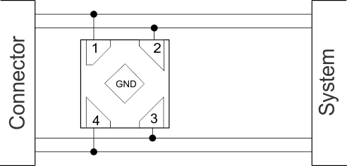
Simplified Schematic
Pinout
4 Revision History
Changes from B Revision (February 2017) to C Revision
- Added "Power Supply Recommendations" sectionGo
Changes from A Revision (December 2015) to B Revision
- Changed the value of RDYN from 0.75 and 0.65 to 0.45 and 0.42 respectively, in the Electrical Characteristics tableGo
Changes from * Revision (May 2014) to A Revision
- Updated the Handling Ratings table into an ESD Ratings table and moved Tstg to the Absolute Maximum Ratings tableGo
- Added new note to Absolute Maximum Ratings table Go
- Added frequency test condition to IO capacitance in the Electrical Characteristics tableGo
- Added Community Resources Go
5 Pin Configuration and Functions
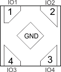
Pin Functions
| PIN | I/O | DESCRIPTION | |
|---|---|---|---|
| NO | NAME | ||
| 1 | IO1 | IO | ESD protected line |
| 2 | IO2 | IO | ESD protected line |
| 3 | IO3 | IO | ESD protected line |
| 4 | IO4 | IO | ESD protected line |
| 5 | GND | — | Ground |
6 Specifications
6.1 Absolute Maximum Ratings
over operating free-air temperature range (unless otherwise noted)(1)(2)(3)| MIN | MAX | UNIT | ||
|---|---|---|---|---|
| Peak pulse | IEC 61000-4-5 Current (tp – 8/20 µs)(4) | 3 | A | |
| IEC 61000-4-5 Power (tp – 8/20 µs)(4) | 40 | W | ||
| Operating temperature | –40 | 125 | °C | |
| Storage temperature | Tstg | –65 | 155 | °C |
6.2 ESD Ratings
| VALUE | UNIT | |||
|---|---|---|---|---|
| V(ESD) | Electrostatic discharge | Human body model (HBM), per ANSI/ESDA/JEDEC JS-001, all pins(1) | ±2000 | V |
| Charged device model (CDM), per JEDEC specification JESD22-C101, all pins(2) | ±500 | |||
6.3 Recommended Operating Conditions
over operating free-air temperature range (unless otherwise noted)| MIN | MAX | UNIT | ||
|---|---|---|---|---|
| VIO | Input pin voltage | –5.5 | 5.5 | V |
| TA | Operating free-air temperature | –40 | 125 | °C |
6.4 Thermal Information
| THERMAL METRIC(1) | TPD4E6B06 | UNIT | |
|---|---|---|---|
| DPW (X2SON) | |||
| 5 PINS | |||
| RθJA | Junction-to-ambient thermal resistance | 291.8 | °C/W |
| RθJC(top) | Junction-to-case (top) thermal resistance | 224.2 | °C/W |
| RθJB | Junction-to-board thermal resistance | 245.8 | °C/W |
| ψJT | Junction-to-top characterization parameter | 31.4 | °C/W |
| ψJB | Junction-to-board characterization parameter | 245.6 | °C/W |
| RθJC(bot) | Junction-to-case (bottom) thermal resistance | 195.4 | °C/W |
6.5 Electrical Characteristics
TA = –40°C to +125°C (unless otherwise specified)| PARAMETER | TEST CONDITION | MIN | TYP | MAX | UNIT | |
|---|---|---|---|---|---|---|
| VRWM | Reverse stand-off voltage | IIO = 10 µA | –5.5 | 5.5 | V | |
| VBRF | Break-down voltage | IIO to GND = 1 mA | 6 | V | ||
| VBRR | Break-down voltage | IGND to IO = 1 mA | 6 | V | ||
| ILEAK | Leakage current | VIO = 5 V | 100 | nA | ||
| VCLAMP | Clamp voltage with ESD strike | I = 1 A, IO to GND, 8/20 μs(1) | 10 | V | ||
| I = 5 A, IO to GND, 8/20 μs(1) | 13 | V | ||||
| I = 1 A, IO to GND, 8/20 μss(1) | 9 | V | ||||
| I = 5 A, IO to GND, 8/20 μs(1) | 13 | V | ||||
| RDYN | Dynamic resistance | Any IO to GND pin(2) | 0.45 | Ω | ||
| GND to any IO pin(2) | 0.42 | Ω | ||||
| CL | IO capacitance | VIO = 2.5 V; ƒ = 10 MHz | 4.8 | 7 | pF | |
6.6 Typical Characteristics




7 Detailed Description
7.1 Overview
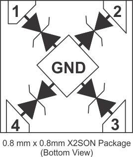
The TPD4E6B06 is a four channel ESD Protection device in an ultra small DPW package. It is the industry’s smallest 4-CH ESD protection device with 0.48-mm pitch. This larger pitch helps save on PCB manufacturing costs. The device provides IEC61000-4-2 compliance up to 15-kV contact discharge. It has an ESD clamp circuit with back-to-back diodes for bipolar/bidirectional signal support. The 4.8-pF (Typical) line capacitance is suitable for a wide range of applications supporting frequencies up to 700 MHz.
7.2 Functional Block Diagram

7.3 Feature Description
7.3.1 IEC 61000-4-2 Level 2 ESD Protection
The IO pins can withstand ESD events up to ±15-kV contact and ±15-kV air. An ESD-surge clamp diverts the current to ground.
7.3.2 IEC 61000-4-5 Surge Protection
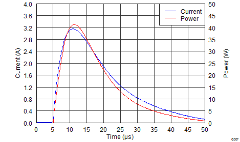
The IO pins can withstand surge events up to 3 A and 40 W (8/20 µs waveform). An ESD-surge clamp diverts this current to ground.
7.3.3 IO Capacitance
The capacitance between any IO pin to ground is 4.8 pF (typical). This capacitance supports frequencies up to 700 MHz.
7.3.4 RDYN
The low RDYN of 0.75 Ω (typical) allows for lower clamping voltages.
7.3.5 DC Breakdown Voltage
The DC breakdown voltage of any IO pin is a minimum of ±6 V. This ensures that sensitive equipment is protected from surges above the reverse standoff voltage of ±5.5 V (minimum).
7.3.6 Ultra-Low Leakage Current
The IO pins feature an ultra-low leakage current of 100 nA (maximum) with a bias of 2.5 V.
7.3.7 Clamping Voltage
The IO pins feature an ESD clamp capable of clamping the voltage to 10 V (IO to GND) or 9 V (GND to IO) of IEC61000-4-5 surge when IPP = 1 A.
7.3.8 Industrial Temperature Range
This device features an industrial operating range of –40°C to +125°C.
7.3.9 Space Saving DPW Package
The small 0.8 mm × 0.8 mm package size saves board space and makes it easy to add ESD protection.
7.4 Device Functional Modes
The TPD4E6B06 is a passive integrated circuit that triggers when voltages are above VBRF or VBRR. During ESD events, voltages as high as ±15 kV (air) can be directed to ground via the internal diode network. Once the voltages on the protected line fall below the trigger levels of the TPD4E6B06 (usually within 10s of nano-seconds) the device reverts to passive.