-
TPD4S009 4-Channel ESD Solution for High-Speed Differential Interface
- 1 Features
- 2 Applications
- 3 Description
- 4 Revision History
- 5 Pin Configuration and Functions
- 6 Specifications
-
7 Detailed Description
- 7.1 Overview
- 7.2 Functional Block Diagram
- 7.3
Feature Description
- 7.3.1 ±8-kV IEC61000-4-2 Level 4 Contact ESD Protection
- 7.3.2 IEC61000-4-5 Surge Protection
- 7.3.3 I/O Capacitance
- 7.3.4 Low Leakage Current
- 7.3.5 Supports High-Speed Differential Data Rates
- 7.3.6 Ultra-low Matching Capacitance Between Differential Signal Pairs
- 7.3.7 Ioff Feature for the TPD4S009
- 7.3.8 Industrial Temperature Range
- 7.3.9 Easy Flow-Through Routing
- 7.4 Device Functional Modes
- 8 Application and Implementation
- 9 Power Supply Recommendations
- 10Layout
- 11Device and Documentation Support
- 12Mechanical, Packaging, and Orderable Information
- IMPORTANT NOTICE
Package Options
Mechanical Data (Package|Pins)
Thermal pad, mechanical data (Package|Pins)
- DRY|6
Orderable Information
TPD4S009 4-Channel ESD Solution for High-Speed Differential Interface
1 Features
- IEC 61000-4-2 Level 4 ESD Protection
- ±8-kV Contact Discharge
- IEC 61000-4-5 Surge Protection
- 2.5A (8/20µs)
- I/O Capacitance: 0.8 pF (Typical)
- Low Leakage Current: 10 nA (Typical)
- Supports High-Speed Differential Data Rates
(3-dB Bandwidth > 4 GHz) - Ultra-low Matching Capacitance Between Differential Signal Pairs
- Ioff Feature for the TPD4S009
- Industrial Temperature Range:
–40°C to 85°C - Easy Straight through Routing, Space-Saving Package Options
2 Applications
- End Equipment
- Set-Top Boxes
- DTVs
- Laptop/Desktop
- Electronic Point of Sale (EPOS)
- Interfaces
- USB 2.0
- HDMI 1.4
- LVDS
- SATA
- Ethernet
- FireWire
3 Description
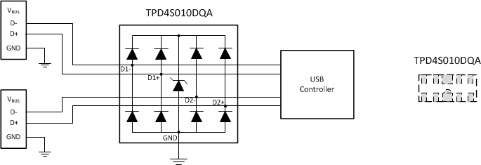
The TPD4S009 and TPD4S010 are four-channel TVS diode arrays for electrostatic discharge (ESD) protection. TPD4S009 and TPD4S010 are rated to dissipate contact ESD strikes at the maximum level specified in the IEC 61000-4-2 international standard (Level 4), with ±8-kV contact discharge ESD protection. The low capacitance (0.8-pF) of these devices, coupled with the excellent matching between differential signal pairs (0.05-pF line-line capacitance for the TPD4S009DRY) enables this device to provide transient voltage suppression circuit protection for high-speed differential data rates (3-dB bandwidth > 4 GHz).
The TPD4S009 is offered in DBV, DCK, DGS, and DRY packages. The TPD4S009DRYR is the most space saving package option available for dual pair high-speed differential lines. The TPD4S010 is offered in the industry standard DQA package. The TPD4S009DGSR and TPD4S010DQAR offer flow-through board layout options to reduce signal glitches normally caused by routing mismatches between the D+ and D- signal pair. See also TPD4E05U06DQAR which is P2P compatible with TPD4S010DQAR. This device offers higher IEC ESD protection, lower capacitance, lower RDYN, lower DC breakdown voltage, and lower clamping voltage.
Device Information(1)
| PART NUMBER | PACKAGE | BODY SIZE (NOM) |
|---|---|---|
| TPD4S009 | SOT (6) | 2.90 mm × 1.60 mm |
| 2.00 mm × 1.25 mm | ||
| VSSOP (10) | 3.00 mm × 3.00 mm | |
| USON (6) | 1.45 mm × 1.00 mm | |
| TPD4S010 | USON (10) | 2.50 mm × 1.00 mm |
- For all available packages, see the orderable addendum at the end of the datasheet.
Simplified Schematic
4 Revision History
Changes from F Revision (August 2013) to G Revision
- Added Pin Configuration and Functions section, ESD Ratings table, Feature Description section, Device Functional Modes, Application and Implementation section, Power Supply Recommendations section, Layout section, Device and Documentation Support section, and Mechanical, Packaging, and Orderable Information section Go
Changes from E Revision (December 2011) to F Revision
- Removed Ordering Information table.Go
5 Pin Configuration and Functions


Pin Functions
6 Specifications
6.1 Absolute Maximum Ratings
over operating free-air temperature range (unless otherwise noted)| MIN | MAX | UNIT | |||
|---|---|---|---|---|---|
| VCC | Supply voltage range for TPD4S009 | –0.3 | 6 | V | |
| VIO | IO signal voltage range | 0 | VCC | V | |
| TA | Characterized free-air operating temperature range | –40 | 85 | °C | |
| Lead temperature, 1.6 mm (1/16 in) from case for 10 s) | 260 | °C | |||
| Peak pulse power (tp = 8/20 μs) | 25 | W | |||
| Peak pulse current (tp = 8/20 μs) | 2.5 | A | |||
| Tstg | Storage temperature range | –65 | 125 | °C | |
6.2 ESD Ratings
| VALUE | UNIT | |||
|---|---|---|---|---|
| V(ESD) | Electrostatic discharge | Human body model (HBM), per ANSI/ESDA/JEDEC JS-001(1) | ±2500 | V |
| Charged-device model (CDM), per JEDEC specification JESD22-C101(2) | ±1500 | |||
| IEC 61000-4-2 Contact Discharge | ±8000 | |||
| IEC 61000-4-2 Air-Gap Discharge | ±9000 | |||
6.3 Recommended Operating Conditions
over operating free-air temperature range (unless otherwise noted)| MIN | NOM | MAX | UNIT | ||
|---|---|---|---|---|---|
| TA Operating free-air Temperature Range | -40 | 85 | °C | ||
| Operating Voltage | VCC Pin | 0.9 | 5.5 | V | |
| IOx Pin (TPD4S009) | 0 | VCC | |||
| IOx Pin (TPD4S010) | 0 | 5.5 | |||
6.4 Thermal Information
| THERMAL METRIC(1) | TPD4S009 | TPD4S010 | UNIT | ||||
|---|---|---|---|---|---|---|---|
| DBV (SOT) | DCK (SOT) | DGS (VSSOP) | DRY (USON) | DQA (USON) | |||
| 6 PINS | 6 PINS | 10 PINS | 6 PINS | 10 PINS | |||
| RθJA | Junction-to-ambient thermal resistance | 201.7 | 254.4 | 205.0 | 380.55 | 265.3 | °C/W |
| RθJC(top) | Junction-to-case (top) thermal resistance | 175.0 | 123.9 | 76.1 | 229.07 | 129.4 | °C/W |
| RθJB | Junction-to-board thermal resistance | 47.6 | 94.0 | 126.0 | 235.57 | 189.7 | °C/W |
| ψJT | Junction-to-top characterization parameter | 52.8 | 14.5 | 9.4 | 56.76 | 31.1 | °C/W |
| ψJB | Junction-to-board characterization parameter | 47.1 | 92.3 | 124.3 | 232.80 | 189.7 | °C/W |
| RθJC(bot) | Junction-to-case (bottom) thermal resistance | N/A | N/A | N/A | 91.03 | N/A | °C/W |
6.5 Electrical Characteristics
over operating free-air temperature range (unless otherwise noted)| PARAMETER | TEST CONDITIONS | MIN | TYP | MAX | UNIT | ||||
|---|---|---|---|---|---|---|---|---|---|
| VRWM | Reverse standoff voltage | Any IO pin to ground | 5.5 | V | |||||
| VBR | Breakdown voltage | IIO = 1 mA | Any IO pin to ground | 9 | V | ||||
| IIO | IO port current | VIO = 3.3 V, VCC = 5 V | Any IO pin | 0.01 | 0.1 | μA | |||
| Ioff | Current from IO port to supply pins | VIO = 3.3 V, VCC = 5 V | Any IO pin | 0.01 | 0.1 | μA | |||
| VD | Diode forward voltage | IIO = 8 mA | Lower clamp diode | 0.6 | 0.8 | 0.95 | V | ||
| RDYN | Dynamic resistance | I = 1 A | Any IO pin | 1.1 | Ω | ||||
| CIO | IO capacitance | VCC = 5 V, VIO = 2.5 V | Any IO pin | 0.8 | pF | ||||
| ICC | Operating supply current | VIO = Open, VCC = 5 V | VCC pin | 0.1 | 1 | μA | |||
6.6 Typical Characteristics
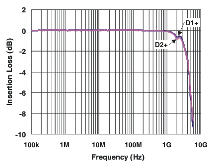 Figure 1. Insertion Loss S21 – I/O to GND
7 Detailed Description
7.1 Overview
The TPD4S009 and TPD4S010 are four-channel TVS diode arrays for electrostatic discharge (ESD) protection. TPD4S009 and TPD4S010 are rated to dissipate contact ESD strikes at the maximum level specified in the IEC 61000-4-2 international standard (Level 4), with ±8-kV contact discharge ESD protection. The low 0.8 pF capacitance of these devices, coupled with the excellent matching between differential signal pairs (0.05-pF line-line capacitance for the TPD4S009DRY) enables this device to operate at high-speed differential data rates (3-dB bandwidth > 4 GHz).
The TPD4S009 offers an optional VCC supply pin which can be connected to system supply plane. There is a blocking diode at the VCC pin to enable the Ioff feature for the TPD4S009. The TPD4S009 can handle live signal at the D+, D- pins when the VCC pin is connected to zero volt. The VCC pin allows all the internal circuit nodes of the TPD4S009 to be at known potential during start up time. However, connecting the optional VCC pin to board supply plane doesn't affect the system level ESD performance of the TPD4S009. The TPD4S010 does not offer the VCC pin.
7.2 Functional Block Diagram
 Figure 6. TPD4S009
 Figure 7. TPD4S010
7.3 Feature Description
7.3.1 ±8-kV IEC61000-4-2 Level 4 Contact ESD Protection
The I/O pins can withstand ESD events up to ±8-kV contact and ±9-kV air. An ESD/surge clamp diverts the current to ground.
7.3.2 IEC61000-4-5 Surge Protection
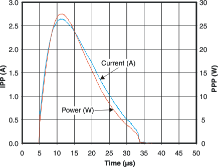
The I/O pins can withstand surge events up to 2.5 A and 25 W (8/20 µs waveform). An ESD/surge clamp diverts this current to ground.
7.3.3 I/O Capacitance
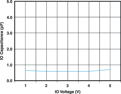
The capacitance between each I/O pin to ground is 0.8 pF (typical) for both TPD4S009 and TPD4S010. These devices support data rates up to 3.4 Gbps.
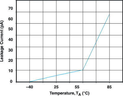
7.3.4 Low Leakage Current
The I/O pins feature a low leakage current of 10 nA (typical) with an IO bias of 3.3 V and VCC bias of 5V.
7.3.5 Supports High-Speed Differential Data Rates
The I/O pins low capacitance of 0.8 pF (typical) gives them a typical –3 dB bandwidth > 4GHz. This allows TPD4S009 and TPD4S010 to protect interfaces with high speed signals like HDMI 1.4.
7.3.6 Ultra-low Matching Capacitance Between Differential Signal Pairs
The monolithic silicon technology allows matching between the differential signal pairs. The excellent matching between the differential pair signal lines (0.05-pF line-line capacitance for the TPD4S009DRY) enables this device to operate at high-speed differential data rates (3-dB bandwidth > 4 GHz). Excellent matching capacitance between differential signal pairs is also crucial to minimize the inter-pair and intra-pair skew between differential signals, which is crucial for many high-speed signal interfaces like HDMI 1.4.
7.3.7 Ioff Feature for the TPD4S009
The TPD4S009 offers an optional VCC supply pin which can be connected to system supply plane. There is a blocking diode at the VCC pin which makes it so the TPD4S009 can handle live signal at the D+, D- pins when the VCC pin is connected to zero volt. This is the Ioff feature, which is crucial for HDMI, as a live signal can be put on the IO pins when the system is powered off. The TPD4S010 does not offer the VCC pin.
7.3.8 Industrial Temperature Range
This device features an industrial operating range of –40°C to 85°C.
7.3.9 Easy Flow-Through Routing
The layout of this device makes it simple and easy to add protection to an existing layout. The packages offers flow-through routing, requiring minimal modification to an existing layout. Flow-through routing also allows the PCB designer to optimize the signal integrity of any high-speed signals being protected.
7.4 Device Functional Modes
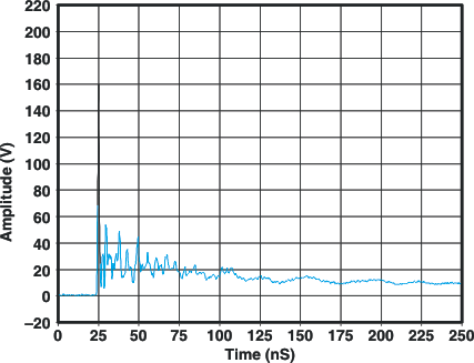
TPD4S009 and TPD4S010 are passive integrated circuits that trigger when voltages are above VBR or below the lower diodes Vf (–0.6 V). During ESD events, voltages as high as ±8 kV (contact) can be directed to ground via the internal diode network. Once the voltages on the protected line fall below the trigger levels of TPD4S009 or TPD4S010 (usually within 10’s of nano-seconds) the device reverts back to its high-impedance state.
8 Application and Implementation
NOTE
Information in the following applications sections is not part of the TI component specification, and TI does not warrant its accuracy or completeness. TI’s customers are responsible for determining suitability of components for their purposes. Customers should validate and test their design implementation to confirm system functionality.
8.1 Application Information
TPD4S009 and TPD4S010 are four-channel TVS diode arrays which are used to provide IEC 61000-4-2 system level ESD protection for a human interface connector. TPD4S009 and TPD4S010 provide a path to ground for dissipating ESD events on hi-speed signal lines between the human interface connector and the system. As the current from ESD passes through the TVS, only a small voltage drop is present across the diode. This is the voltage presented to the protected IC. The low RDYN of the triggered TVS holds this voltage, VCLAMP, to a safe level for the protected IC.
8.2 Typical Application
 Figure 8. Typical Application Schematic
8.2.1 Design Requirements
For this design example, two TPD4S010 devices, and one TPD5S116 are being used in an HDMI 1.4 application. This will provide a complete port protection scheme.
Given the HDMI 1.4 application, the following parameters are known.
| DESIGN PARAMETER | VALUE |
|---|---|
| Signal range on Pins 1, 2, 4, or 5 | 0 V to 3.6 V |
| Operating Frequency | 1.7 GHz |
8.2.2 Detailed Design Procedure
To begin the design process, some parameters must be decided upon; the designer needs to know the following:
- Signal range on all the protected lines
- Operating frequency
8.2.2.1 Signal Range on Pin 1, 2, 4, or 5
TPD4S010 has 4 identical protection channels for signal lines. The symmetry of the device provides flexibility when selecting which of the 4 I/O channels will protect which signal lines. Any I/O will support a signal range of 0 to 5.5 V. Therefore, this device will support the HDMI 1.4 signal swing.
8.2.2.2 Bandwidth on Pin 1, 2, 4, or 5
Each pin of the TPD4S010 has a typical –3 dB bandwidth of 4GHz. Therefore, this device can handle HDMI 1.4 data rate of 3.4 Gbps with operating frequency of 1.7 GHz.

