SLVSF72C December 2019 – February 2021 TPD4S311 , TPD4S311A
PRODUCTION DATA
- 1 Features
- 2 Applications
- 3 Description
- 4 Revision History
- 5 Device Comparison Table
- 6 Pin Configuration and Functions
- 7 Specifications
-
8 Detailed Description
- 8.1 Overview
- 8.2 Functional Block Diagram
- 8.3
Feature Description
- 8.3.1 4-Channels of Short-to-VBUS Overvoltage Protection (CC1, CC2, SBU1, SBU2 Pins ): 24-VDC Tolerant
- 8.3.2 4-Channels of IEC 61000-4-2 ESD Protection (CC1, CC2, SBU1, SBU2 Pins)
- 8.3.3 CC1, CC2 Overvoltage Protection FETs 400-mA or 600-mA Capable for Passing VCONN Power
- 8.3.4 CC Dead Battery Resistors Integrated for Handling the Dead Battery Use Case in Mobile Devices
- 8.3.5 1.69-mm × 1.69-mm DSBGA Package
- 8.4 Device Functional Modes
- 9 Application and Implementation
- 10Power Supply Recommendations
- 11Layout
- 12Device and Documentation Support
- 13Mechanical, Packaging, and Orderable Information
Package Options
Mechanical Data (Package|Pins)
- YBF|16
Thermal pad, mechanical data (Package|Pins)
Orderable Information
7.8 Typical Characteristics
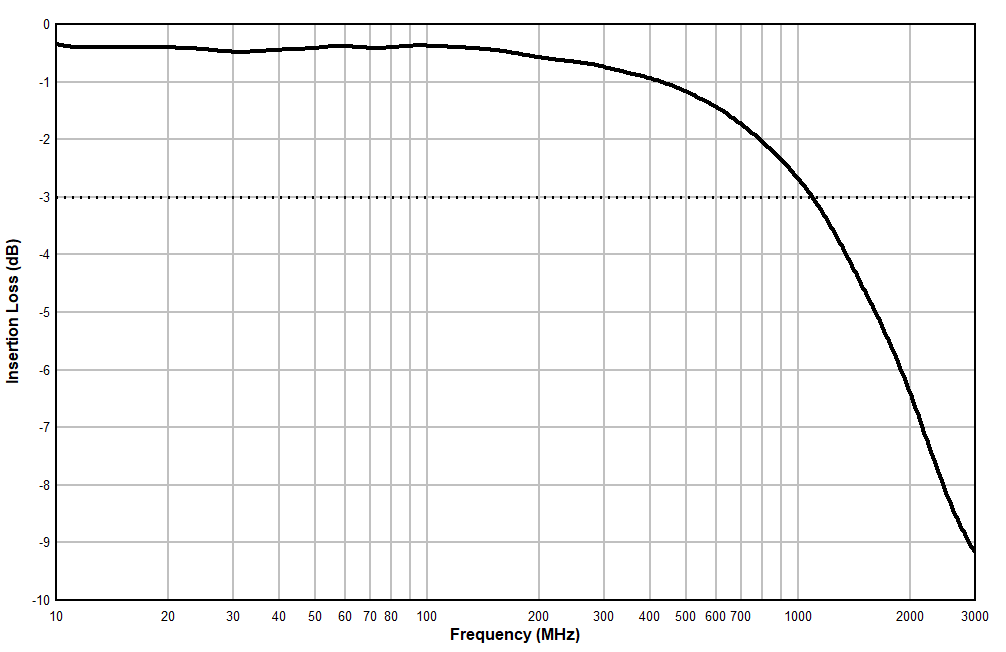 Figure 7-1 SBU Bandwidth
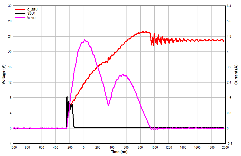 Figure 7-3 SBU
Short-to-VBUS 24 V Zoomed In
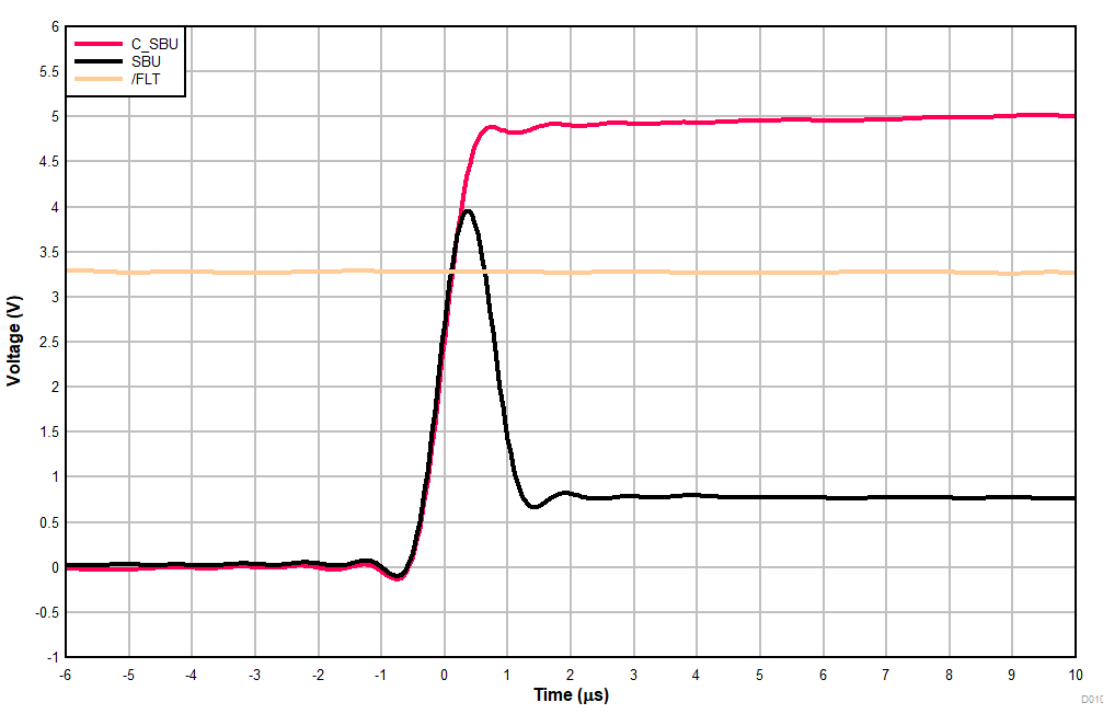 Figure 7-5 SBU Short-to-VBUS 5 V Zoomed In
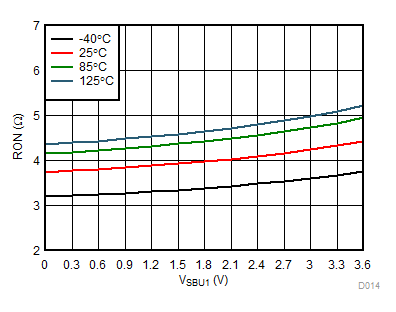 Figure 7-7 SBU RON Flatness
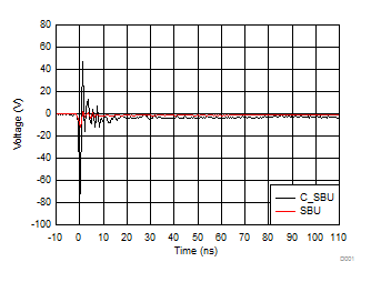 Figure 7-9 SBU IEC 61000-4-2 –4-kV Response Waveform
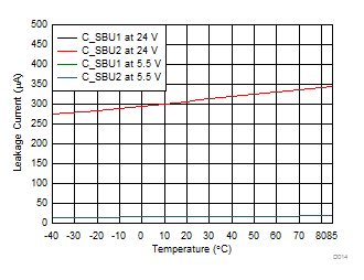 Figure 7-11 C_SBU OVP Leakage Current vs Ambient Temperature at 5.5 V and 24 V
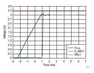 Figure 7-13 SBU FET Turnon Timing
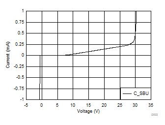 Figure 7-15 SBU
IV Curve
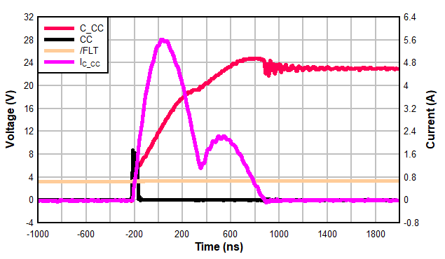 Figure 7-17 CC
Short-to-VBUS 24 V Zoomed In
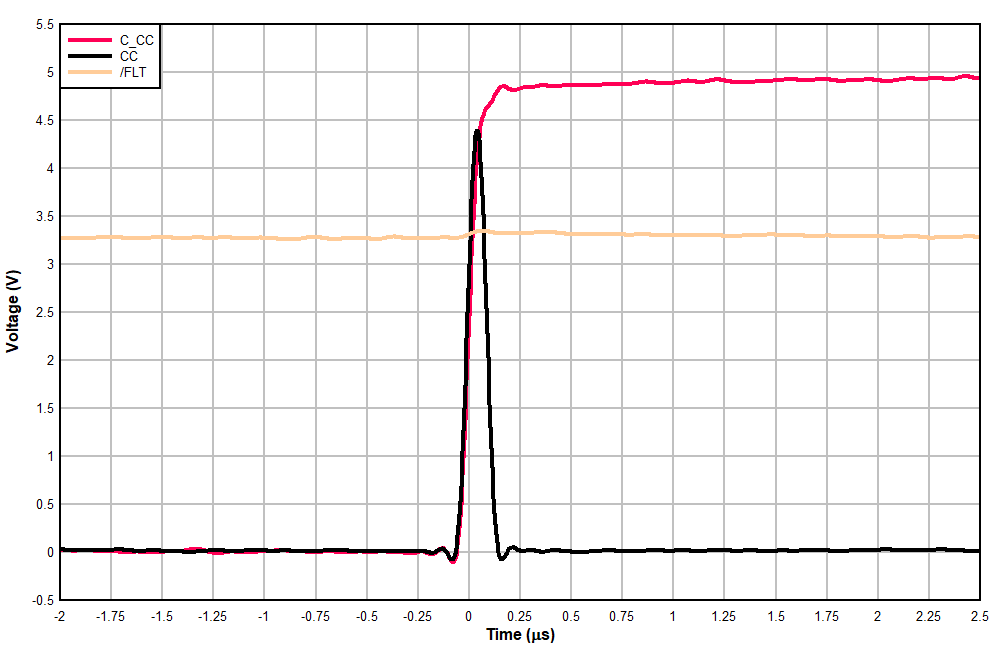 Figure 7-19 CC Short-to-VBUS 5 V Zoomed In
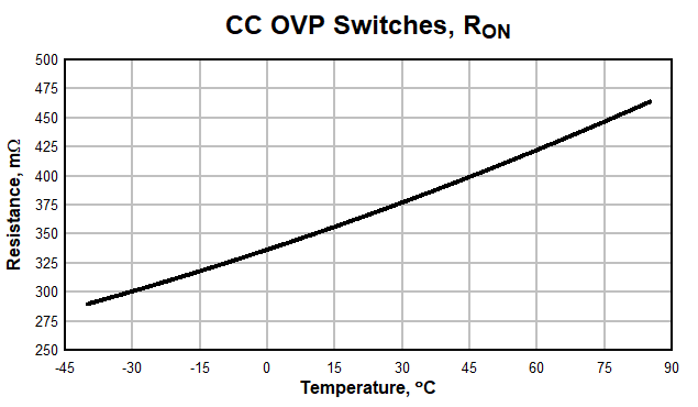 Figure 7-21 CC RON Versus Temperature
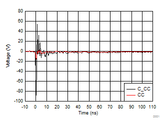 Figure 7-23 CC IEC 61000-4-2 –8-kV Response Waveform
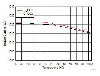 Figure 7-25 C_CC OVP Leakage Current vs Ambient Temperature at C_CC = 24 V
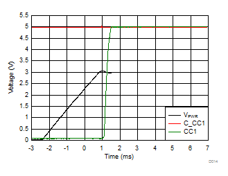 Figure 7-27 CC FET Turnon Timing
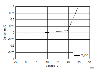 Figure 7-29 C_CC IV Curve
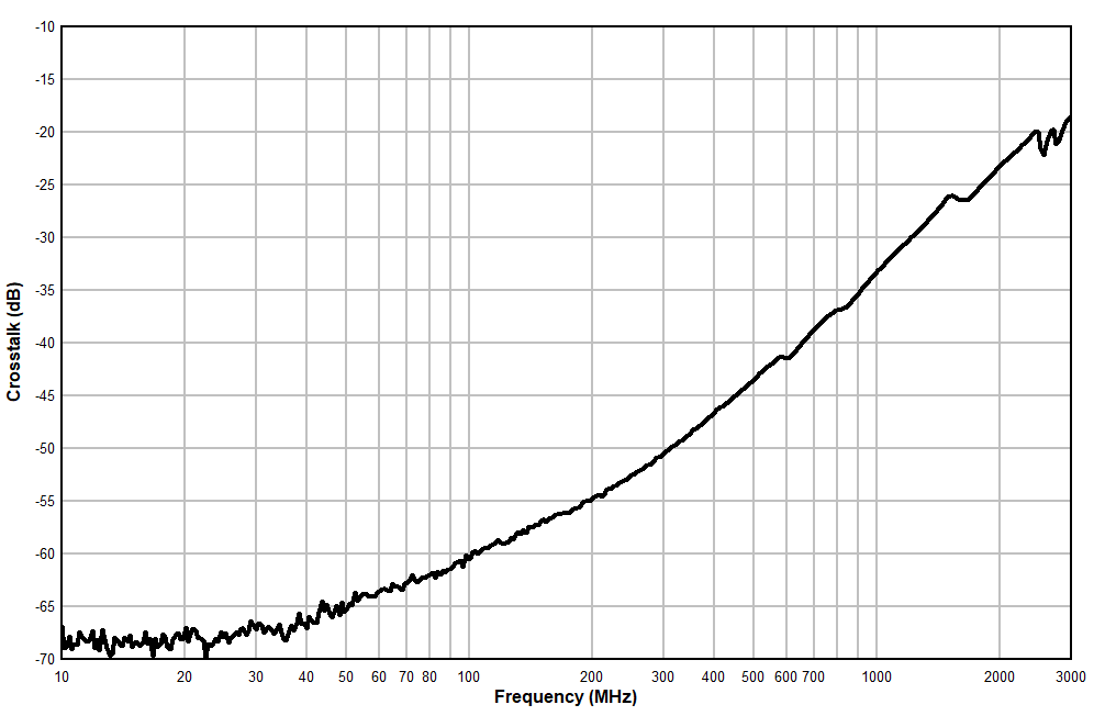 Figure 7-2 SBU Crosstalk
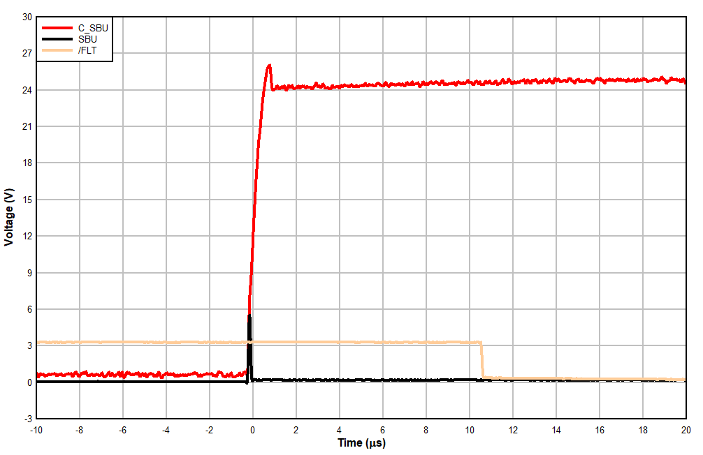 Figure 7-4 SBU
Short-to-VBUS 24 V Zoomed Out
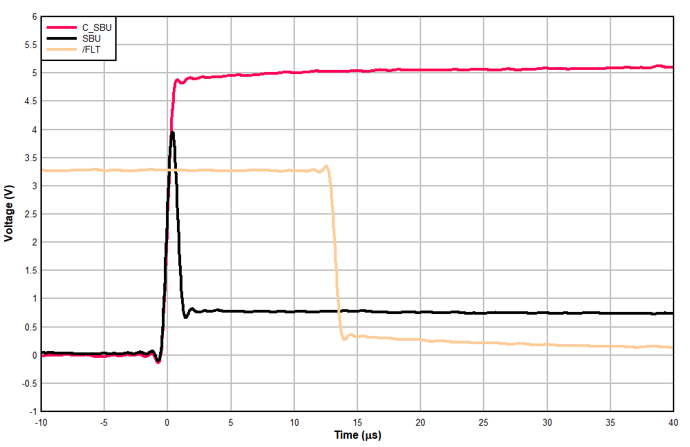 Figure 7-6 SBU Short-to-VBUS 5 V Zoomed Out
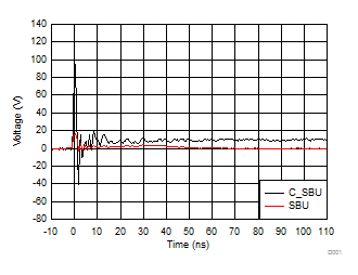 Figure 7-8 SBU IEC 61000-4-2 4-kV Response Waveform
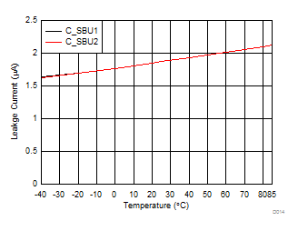 Figure 7-10 SBU Path Leakage Current vs Ambient Temperature at 3.6 V
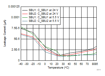 Figure 7-12 SBU OVP Leakage Current vs Ambient Temperature at 5.5 V and 24 V
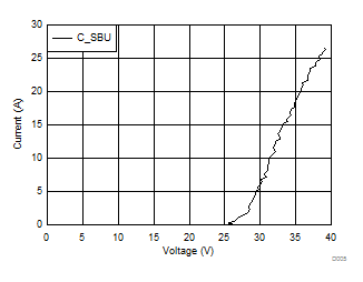 Figure 7-14 C_SBU TLP Curve Unpowered
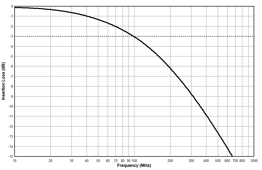 Figure 7-16 CC Bandwidth
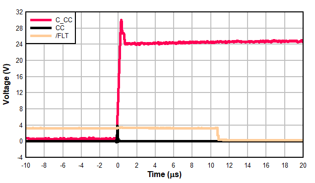 Figure 7-18 CC
Short-to-VBUS 24 V Zoomed Out
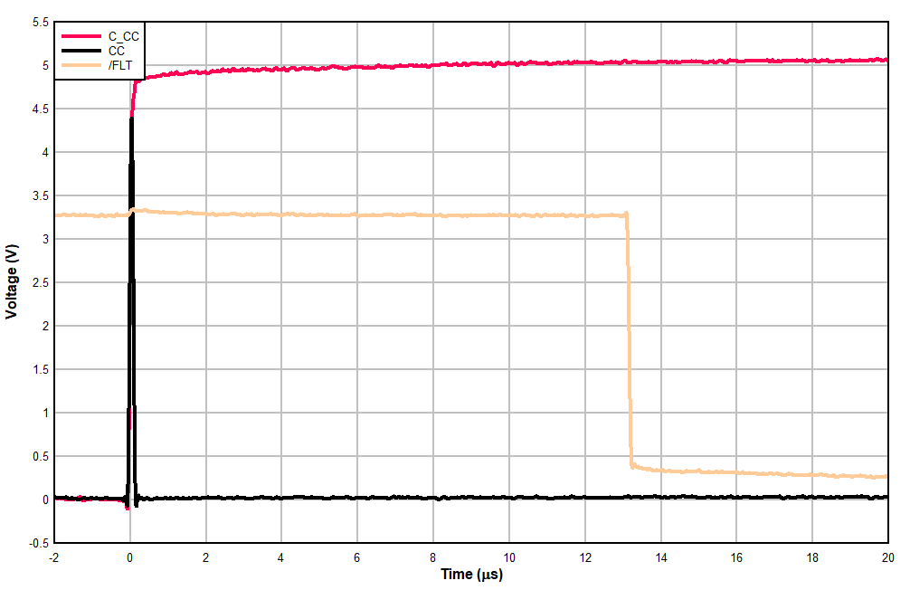 Figure 7-20 CC Short-to-VBUS 5 V Zoomed Out
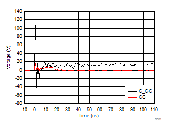 Figure 7-22 CC
IEC 61000-4-2 8-kV Response Waveform
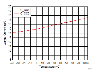 Figure 7-24 C_CC Path Leakage Current vs Ambient Temperature at C_CC = 5.5 V
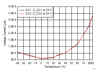 Figure 7-26 CC OVP Leakage Current vs Ambient Temperature at C_CC = 24 V
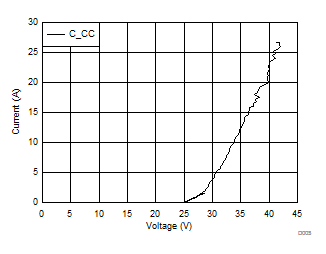 Figure 7-28 C_CC TLP Curve Unpowered
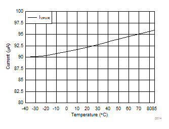 Figure 7-30 VPWR Supply Leakage vs Ambient Temperature at 3.6 V