SLVSF72C December 2019 – February 2021 TPD4S311 , TPD4S311A
PRODUCTION DATA
- 1 Features
- 2 Applications
- 3 Description
- 4 Revision History
- 5 Device Comparison Table
- 6 Pin Configuration and Functions
- 7 Specifications
-
8 Detailed Description
- 8.1 Overview
- 8.2 Functional Block Diagram
- 8.3
Feature Description
- 8.3.1 4-Channels of Short-to-VBUS Overvoltage Protection (CC1, CC2, SBU1, SBU2 Pins ): 24-VDC Tolerant
- 8.3.2 4-Channels of IEC 61000-4-2 ESD Protection (CC1, CC2, SBU1, SBU2 Pins)
- 8.3.3 CC1, CC2 Overvoltage Protection FETs 400-mA or 600-mA Capable for Passing VCONN Power
- 8.3.4 CC Dead Battery Resistors Integrated for Handling the Dead Battery Use Case in Mobile Devices
- 8.3.5 1.69-mm × 1.69-mm DSBGA Package
- 8.4 Device Functional Modes
- 9 Application and Implementation
- 10Power Supply Recommendations
- 11Layout
- 12Device and Documentation Support
- 13Mechanical, Packaging, and Orderable Information
Package Options
Mechanical Data (Package|Pins)
- YBF|16
Thermal pad, mechanical data (Package|Pins)
Orderable Information
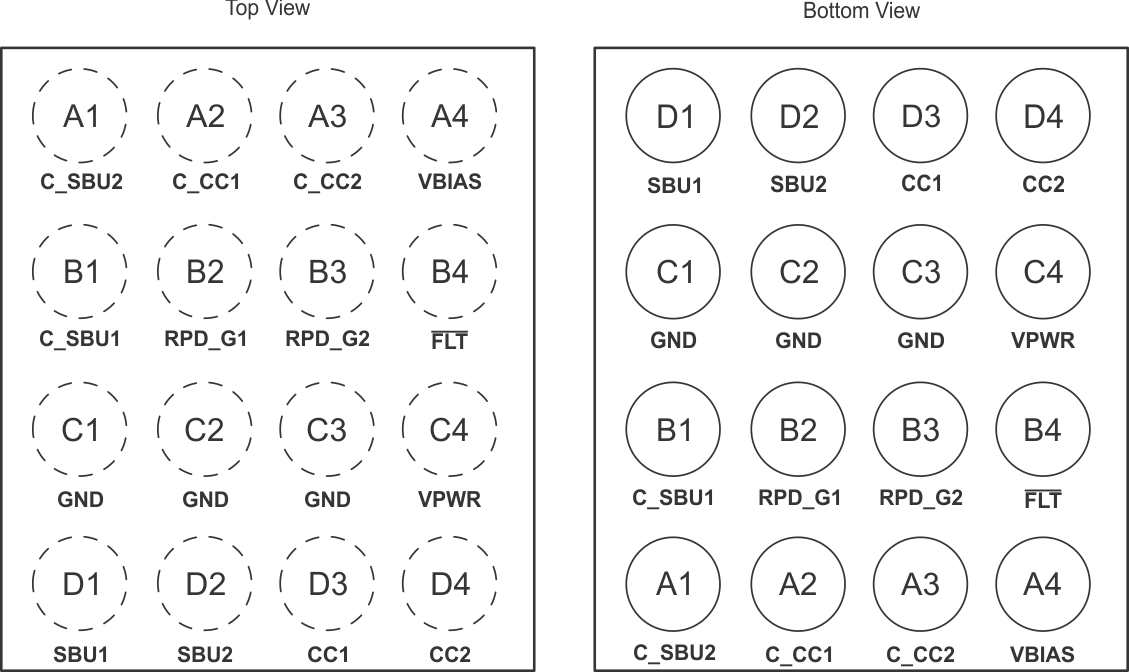
6 Pin Configuration and Functions
 Figure 6-1 YBF
Package16-Pin DSBGA
Figure 6-1 YBF
Package16-Pin DSBGATable 6-1 Pin Functions
| PIN | TYPE(1) | DESCRIPTION | |
|---|---|---|---|
| NO. | NAME | ||
| A1 | C_SBU2 | I/O | Connector side of the SBU2 OVP FET. Connect to either SBU pin of the USB Type-C connector. |
| A2 | C_CC1 | I/O | Connector side of the CC1 OVP FET. Connect to either CC pin of the USB Type-C connector. |
| A3 | C_CC2 | I/O | Connector side of the CC2 OVP FET. Connect to either CC pin of the USB Type-C connector. |
| A4 | VBIAS | P | Pin for ESD support capacitor. Place a 0.1-µF capacitor on this pin to ground. |
| B1 | C_SBU1 | I/O | Connector side of the SBU1 OVP FET. Connect to either SBU pin of the USB Type-C connector. |
| B2 | RPD_G1 | I/O | Short to C_CC1 if dead battery resistors are needed. If dead battery resistors are not needed, short pin to GND. |
| B3 | RPD_G2 | I/O | Short to C_CC2 if dead battery resistors are needed. If dead battery resistors are not needed, short pin to GND. |
| B4 | FLT | O | Open drain for fault reporting. |
| C1, C2, C3 | GND | GND | Ground |
| C4 | VPWR | P | 2.7-V to 4.5-V power supply. |
| D1 | SBU1 | I/O | System side of the SBU1 OVP FET. Connect to either SBU pin of the SBU MUX. |
| D2 | SBU2 | I/O | System side of the SBU2 OVP FET. Connect to either SBU pin of the SBU MUX. |
| D3 | CC1 | I/O | System side of the CC1 OVP FET. Connect to either CC pin of the CC/PD controller. |
| D4 | CC2 | I/O | System side of the CC2 OVP FET. Connect to either CC pin of the CC/PD controller. |
(1) I = input, O = output, I/O =
input and output, GND = ground, P = power