SLLS685D July 2006 – September 2015 TPD6E001
PRODUCTION DATA.
- 1 Features
- 2 Applications
- 3 Description
- 4 Revision History
- 5 Pin Configuration and Functions
- 6 Specifications
- 7 Detailed Description
- 8 Application and Implementation
- 9 Power Supply Recommendations
- 10Layout
- 11Device and Documentation Support
- 12Mechanical, Packaging, and Orderable Information
Package Options
Mechanical Data (Package|Pins)
Thermal pad, mechanical data (Package|Pins)
- RSF|12
Orderable Information
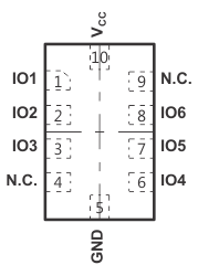
5 Pin Configuration and Functions
RSE Package
10-Pin UQFN
Top View

N.C.- Not internally connected
RSF Package
12-Pin WQFN
Top View

N.C.- Not internally connected
Pin Functions
| PIN | TYPE | DESCRIPTION | ||
|---|---|---|---|---|
| NAME | RSE | RSF | ||
| GND | 5 | 5 | GND | Ground |
| IOx | 1, 2, 3, 6, 7, 8 |
1, 2, 3, 7, 8, 9 |
I/O | ESD-protected channel |
| N.C. | 4, 9 | 4, 6, 10, 12 | — | Not internally connected |
| VCC | 10 | 11 | Power | Power-supply input. Bypass VCC to GND with a 0.1-μF ceramic capacitor. |
| EP | – | EP | GND | Exposed pad. Connect to GND. |