SLLS799C february   2008  – july 2023 TPD6E004

PRODUCTION DATA  

  1.   1
  2. Features
  3. Applications
  4. Description
  5. Revision History
  6. Pin Configuration and Functions
  7. Specifications
    1. 6.1 Absolute Maximum Ratings #GUID-506F33E9-2D36-4FA4-A00D-A85E2C505B35/SLLS7994401
    2. 6.2 ESD Ratings
    3. 6.3 ESD Ratings – Surge Protection
    4. 6.4 Recommended Operating Conditions
    5. 6.5 Thermal Information
    6. 6.6 Electrical Characteristics
    7. 6.7 Typical Characteristics
  8. Detailed Description
    1. 7.1 Overview
    2. 7.2 Functional Block Diagram
    3. 7.3 Feature Description
    4. 7.4 Device Functional Modes
  9. Application and Implementation
    1. 8.1 Application Information
    2. 8.2 Typical Application
      1. 8.2.1 Design Requirements
      2. 8.2.2 Detailed Design Procedure
      3. 8.2.3 Application Curve
    3. 8.3 Power Supply Recommendations
    4. 8.4 Layout
      1. 8.4.1 Layout Guidelines
      2. 8.4.2 Layout Example
  10. Device and Documentation Support
    1. 9.1 Documentation Support
      1. 9.1.1 Related Documentation
    2. 9.2 Support Resources
    3. 9.3 Trademarks
    4. 9.4 Electrostatic Discharge Caution
    5. 9.5 Glossary
  11. 10Mechanical, Packaging, and Orderable Information

Package Options

Mechanical Data (Package|Pins)
Thermal pad, mechanical data (Package|Pins)
Orderable Information

Application Curve

Figure 8-2 is a capture of the voltage clamping waveform of the TPD6E004 during a +8-kV contact IEC 61000-4-2 ESD strike.
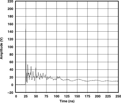
GUID-9D477F84-9C23-4CF6-80C8-35DAD38E48F7-low.gif Figure 8-2 IEC 61000-4-2 +8-kV Contact ESD Clamping Waveform