TPDxF003 Four-, Six-, and Eight-Channel EMI Filters With Integrated ESD Protection
1 Features
- Four-, Six-, and Eight-Channel EMI Filtering for Data Ports
- –3 dB Bandwidth of 200 MHz
- Greater than 25 dB attenuation at 1 GHz
- IEC 61000-4-2 Level 4 ESD Protection
- ±12-kV Contact Discharge
- ±20-kV Air Gap Discharge
- Pi-Style (C-R-C) Filter Configuration
(R = 100 Ω, CTOTAL = 17 pF) - Low 10-nA Leakage Current
- Easy Flow-Through Routing
2 Applications
- Display Interfaces
- Cell Phones
- Tablets
- SVGA Video Connections
- Memory Interfaces
3 Description
The TPDxF003 family is a series of highly integrated devices designed to provide Electromagnetic Interference (EMI) filtering in all systems subjected to electromagnetic interference. These filters also provide a Transient Voltage Suppressor (TVS) diode circuit for Electrostatic Discharge (ESD) protection which prevents damage to the application when subjected to ESD stress far exceeding IEC 61000-4-2 (Level 4).
The TPDxF003 family is specified for –40°C to 85°C operation. These filters are also packaged in space-saving 0.4-mm pitch DQD packages.
Device Information(1)
| PART NUMBER | PACKAGE | BODY SIZE (NOM) |
|---|---|---|
| TPD4F003 | WSON (8) | 1.70 mm x 1.35 mm |
| TPD6F003 | WSON (12) | 2.50 mm x 1.35 mm |
| TPD8F003 | WSON (16) | 3.30 mm x 1.35 mm |
- For all available packages, see the orderable addendum at the end of the datasheet.
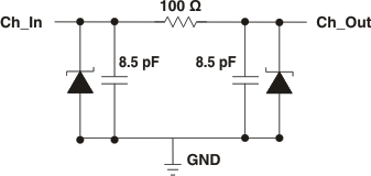
Equivalent Schematic
4 Revision History
Changes from D Revision (January 2010) to E Revision
- Added Handling Rating table, Feature Description section, Device Functional Modes, Application and Implementation section, Power Supply Recommendations section, Layout section, Device and Documentation Support section, and Mechanical, Packaging, and Orderable Information section Go
5 Pin Configuration and Functions
Pin Functions - TPD4F003
| PIN | I/O | DESCRIPTION | |
|---|---|---|---|
| NAME | No. | ||
| ChX_In | 1, 2, 3, 4 | IO | ESD-protected channel, connected to corresponding ChX_Out |
| ChX_Out | 5, 6, 7, 8 | IO | ESD-protected channel, connected to corresponding ChX_In |
| GND | GND | G | Ground |
Pin Functions - TPD6F003
| PIN | I/O | Description | |
|---|---|---|---|
| Name | No. | ||
| ChX_In | 1, 2, 3, 4, 5, 6 | IO | ESD-protected channel, connected to corresponding ChX_Out |
| ChX_Out | 7, 8, 9, 10, 11, 12 | IO | ESD-protected channel, connected to corresponding ChX_In |
| GND | GND | G | Ground |
Pin Functions - TPD8F003
| PIN | I/O | Description | |
|---|---|---|---|
| Name | No. | ||
| ChX_In | 1, 2, 3, 4, 5, 6, 7, 8 | IO | ESD-protected channel, connected to corresponding ChX_Out |
| ChX_Out | 9, 10, 11, 12, 13, 14, 15, 16 | IO | ESD-protected channel, connected to corresponding ChX_In |
| GND | GND | G | Ground |
6 Specifications
6.1 Absolute Maximum Ratings(1)
over operating free-air temperature range (unless otherwise noted)| MIN | MAX | UNIT | |||
|---|---|---|---|---|---|
| VIO | IO to GND | 6 | V | ||
| TJ | Junction temperature | 150 | °C | ||
6.2 Handling Ratings
| MIN | MAX | UNIT | |||
|---|---|---|---|---|---|
| Tstg | Storage temperature range | –65 | 150 | °C | |
| V(ESD) | Electrostatic discharge | Human body model (HBM), per ANSI/ESDA/JEDEC JS-001, all pins(1) | ±15 | kV | |
| Charged device model (CDM), per JEDEC specification JESD22-C101, all pins(2) | ±1500 | V | |||
| IEC 61000-4-2 ESD Rating - Contact | ±12 | kV | |||
| IEC 61000-4-2 ESD Rating - Air | ±20 | ||||
6.3 Recommended Operating Conditions
over operating free-air temperature range (unless otherwise noted)| MIN | MAX | UNIT | ||
|---|---|---|---|---|
| VIO | 0 | 5.5 | V | |
| TA | –40 | 85 | °C | |
6.4 Thermal Information
| THERMAL METRIC(1) | TPD4F003 | TPD6F003 | TPD8F003 | UNIT | |
|---|---|---|---|---|---|
| DQD | |||||
| 8 PINS | 12 PINS | 16 PINS | |||
| RθJA | Junction-to-ambient thermal resistance | 115.6 | 89.2 | 80.8 | °C/W |
| RθJC(top) | Junction-to-case (top) thermal resistance | 108.5 | 100.1 | 88.3 | |
| RθJB | Junction-to-board thermal resistance | 66.4 | 50.5 | 45.8 | |
| ψJT | Junction-to-top characterization parameter | 6.8 | 9.4 | 9.2 | |
| ψJB | Junction-to-board characterization parameter | 65.9 | 50.0 | 45.4 | |
| RθJC(bot) | Junction-to-case (bottom) thermal resistance | 33.2 | 31.0 | 31.8 | |
6.5 Electrical Characteristics
TA = –40°C to 85°C (unless otherwise noted)| PARAMETER | TEST CONDITIONS | MIN | TYP(1) | MAX | UNIT | |
|---|---|---|---|---|---|---|
| VBR | DC breakdown voltage | IIO = 10 μA | 6 | V | ||
| R | Resistance | 85 | 100 | 115 | Ω | |
| C | Capacitance (C1 or C2) | VIO = 2.5 V | 8.5 | pF | ||
| IIO | Channel leakage current | VIO = 3.3 V | 10 | nA | ||
| fC | Cut-off frequency | ZSOURCE = 50 Ω, ZLOAD = 50 Ω | 200 | MHz | ||
6.6 Typical Characteristics
6.6.1 IEC Clamping Waveforms
(clamp voltage measured both at Ch_Out and Ch_In)
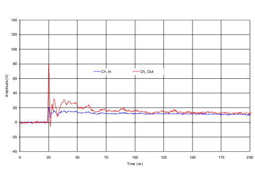 Figure 1. With 8 kV Contact ESD Stress at Ch_Out
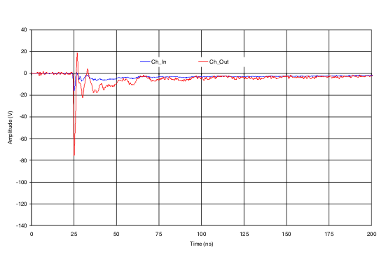 Figure 3. With -8 kV Contact ESD Stress at Ch_Out
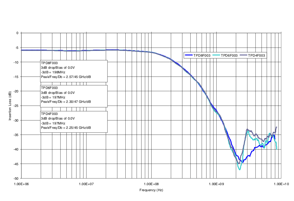
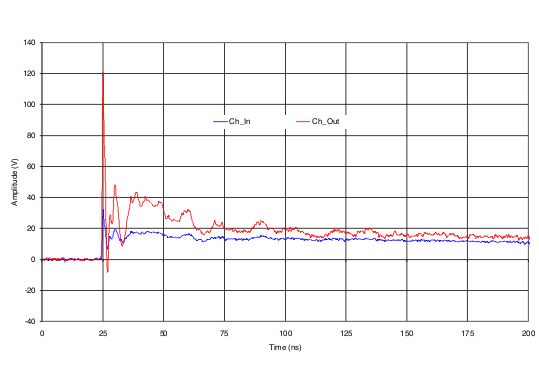 Figure 2. With 12 kV Contact ESD Stress at Ch_Out
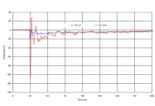 Figure 4. With -12 kV Contact ESD Stress at Ch_Out
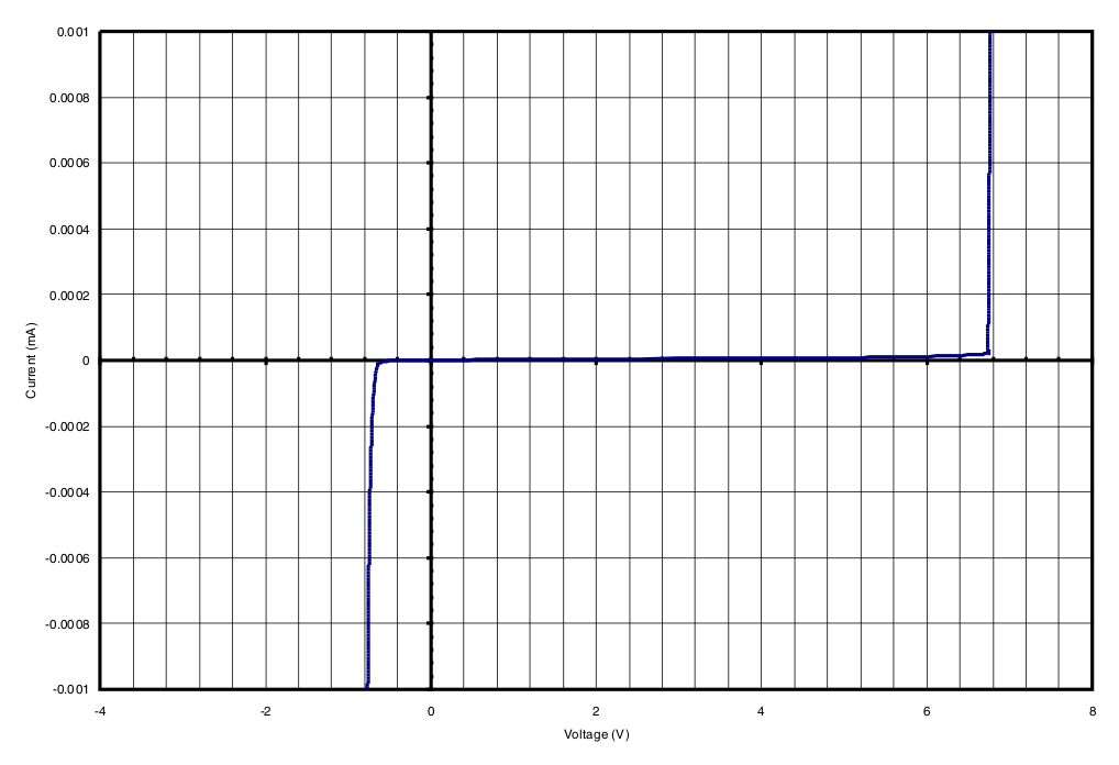 Figure 6. DC Voltage-Current Sweep Across Input/Output Pins
6.6.2 Channel-to-Channel Crosstalk
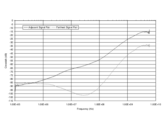 Figure 7. TPD4F003
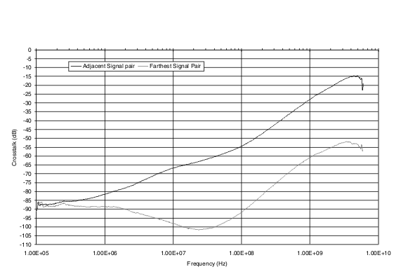 Figure 9. TPD8F003
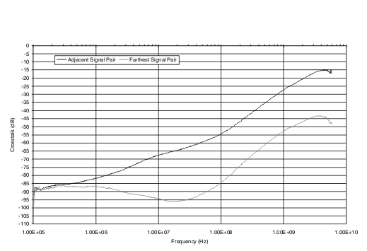 Figure 8. TPD6F003
7 Detailed Description
7.1 Overview
The TPDxF003 family is a series of highly integrated devices designed to provide EMI filtering in all systems subjected to electromagnetic interference. These filters also provide a Transient Voltage Suppressor (TVS) diode circuit for ESD protection which prevents damage to the application when subjected to ESD stress far exceeding IEC 61000-4-2 (Level 4).
7.2 Functional Block Diagram
7.3 Feature Description
The TPDxF003 family is a line of ESD and EMI filtering devices designed to reduce EMI emissions and provide system level ESD protection. Each device can dissipate ESD strikes above the maximum level specified by IEC 61000-4-2 international standard. Additionally, the EMI filtering structure reduces EMI emissions by providing high frequency roll-off.
7.3.1 Four-, Six-, and Eight-Channel EMI Filtering for Data Ports
These devices provide EMI filtering for four, six, or eight channels of data lines.
7.3.2 –3 dB Bandwidth of 200 MHz
These devices have a through –3dB bandwidth of 200 MHz.
7.3.3 Greater Than 25 dB Attenuation at 1 GHz
Signal attenuation is above 25dB at 1 GHz, which provides significant reduction in spurious emissions.
7.3.4 Robust ESD Protection Exceeds IEC 61000-4-2
The ESD protection on all pins exceeds the IEC 61000-4-2 level 4 standard. Contact ESD is rated at ±12 kV and Air-gap ESD is rated at ±20 kV.
7.3.5 Pi-Style (C-R-C) Filter Configuration
This family of devices has a pi-style filtering configuration composed of a series resistor and two capacitors in parallel with the I/O pins. The typical resistor value is 100 Ω and the typical capacitor values are 8.5 pF each.
7.3.6 Low 10-nA Leakage Current
The I/O pins feature an ultra-low leakage current of 10-nA (typical) with a bias of 3.3 V.
7.3.7 Easy Flow-Through Routing
The layout of this device makes it easy to add protection to existing layouts. The packages offer flow-through routing which requires minimal changes to existing layout for addition of these devices.
7.4 Device Functional Modes
The TPDxF003 family of devices are passive integrated circuits that passively filter EMI and trigger when voltages are above VBR or below the lower diode voltage (–0.6 V). During ESD events, voltages as high as ±20 kV (air) can be directed to ground via the internal diode network. Once the voltages on the protected line fall below the trigger levels, the device reverts to passive.