SLIS113E October 2004 – May 2022 TPIC1021
PRODUCTION DATA
- 1 Features
- 2 Applications
- 3 Description
- 4 Revision History
- 5 Description (continued)
- 6 Pin Configuration and Functions
- 7 Specifications
- 8 Detailed Description
- 9 Application and Implementation
- 10Device and Documentation Support
- 11Mechanical, Packaging, and Orderable Information
Package Options
Refer to the PDF data sheet for device specific package drawings
Mechanical Data (Package|Pins)
- D|8
Thermal pad, mechanical data (Package|Pins)
Orderable Information
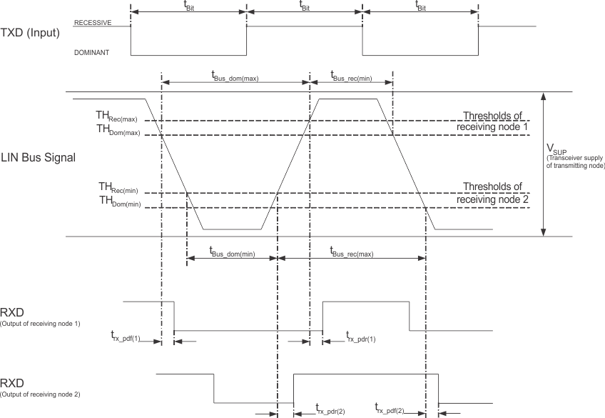
7.6 Timing Requirements
| MIN | NOM | MAX | UNIT | |||
|---|---|---|---|---|---|---|
| D1 | Duty cycle 1(1)(2) | THREC(max) = 0.744×VSUP, THDOM(max) = 0.581×VSUP, VSUP = 7.0 V to 18 V, tBIT = 50 µs (20 kbps), See Figure 7-1 | 0.396 | |||
| D2 | Duty cycle 2(1)(2) | THREC(max) = 0.284×VSUP, THDOM(max) = 0.422×VSUP, VSUP = 7.6 V to 18 V, tBIT = 50 µs (20 kbps), See Figure 7-1 | 0.581 | |||
| D3 | Duty cycle 3(1)(2) | THREC(max) = 0.778×VSUP, THDOM(max) = 0.616×VSUP, VSUP = 7.0 V to 18 V, tBIT = 96 µs (10.4 kbps), See Figure 7-1 | 0.417 | |||
| D4 | Duty cycle 4(1)(2) | THREC(max) = 0.251×VSUP, THDOM(max) = 0.389×VSUP, VSUP = 7.6 V to 18 V, tBIT = 96 µs (10.4 kbps), See Figure 7-1 | 0.590 | |||
| trx_pdr | Receiver rising propagation delay time | RL = 2.4 kΩ, CL = 20 pF, See Figure 7-1 | 6 | µs | ||
| trx_pdf | Receiver rising propagation delay time | RL = 2.4 kΩ, CL = 20 pF, See Figure 7-1 | 6 | µs | ||
| trx_sym | Symmetry of receiver propagation delay time (rising edge) | with respect to falling edge, See Figure 7-1 | –2 | 2 | µs | |
| tNWake | NWake filter time for local wake-up | See Figure 7-1 | 25 | 50 | 100 | µs |
| tLINBUS | LIN wake-up filter time (dominant time for wake-up via LIN bus) | See Figure 7-1 | 25 | 50 | 100 | µs |
| tDST | Dominant state timeout(3) | See Figure 7-1 | 6 | 9 | 14 | ms |
(1) Duty cycle = tBUS_rec(min)/ (2×tBIT)
(2) Duty Cycles: LIN Driver bus load conditions (CLINBUS, RLINBUS): Load1 = 1 nF, 1 kΩ; Load2 = 6.8 nF, 660 Ω; Load3 = 10 nF, 500 Ω. Duty Cycles 3 and 4 are defined for 10.4 kbps operation. The TPIC1021 also meets these lower speed requirements, while it is capable of the higher speed 20.0 kbps operation as specified by Duty Cycles 1 and 2. SAEJ2602 derives propagation delay equations from the LIN 2.0 duty cycle definitions (LIN 2.1 compatible), for details please refer to the SAEJ2602 specification.
(3) Dominant state timeout will limit the minimum data rate to 2.4 kbps.
 Figure 7-1 Definition of Bus Timing Parameters