SLIS117C August   2007  – May 2022 TPIC1021A-Q1

PRODUCTION DATA  

  1. Features
  2. Applications
  3. Description
  4. Revision History
  5. Description (continued)
  6. Device Comparison Table
  7. Pin Configuration and Functions
  8. Specifications
    1. 8.1 Absolute Maximum Ratings
    2. 8.2 ESD Ratings
    3. 8.3 Recommended Operating Conditions
    4. 8.4 Thermal Information
    5. 8.5 Electrical Characteristics
    6. 8.6 Typical Characteristics
  9. Parameter Measurement Information
    1. 9.1 Test Circuit
  10. 10Detailed Description
    1. 10.1 Overview
    2. 10.2 Functional Block Diagram
    3. 10.3 Feature Description
      1. 10.3.1 Local Interconnect Network (LIN) Bus
        1. 10.3.1.1 Transmitter Characteristics
        2. 10.3.1.2 Receiver Characteristics
      2. 10.3.2 Transmit Input (TXD)
        1. 10.3.2.1 TXD Dominant State Time-Out
      3. 10.3.3 Receive Output (RXD)
        1. 10.3.3.1 RXD Wake-up Request
      4. 10.3.4 Supply Voltage (VSUP)
      5. 10.3.5 Ground (GND)
      6. 10.3.6 Enable Input (EN)
      7. 10.3.7 NWake Input (NWake)
      8. 10.3.8 Inhibit Output (INH)
    4. 10.4 Device Functional Modes
      1. 10.4.1 Operating States
        1. 10.4.1.1 Normal Mode
        2. 10.4.1.2 Sleep Mode
          1. 10.4.1.2.1 Wake-Up Events
        3. 10.4.1.3 Standby Mode
  11. 11Application and Implementation
    1. 11.1 Application Information
    2. 11.2 Typical Application
      1. 11.2.1 Design Requirements
      2. 11.2.2 Detailed Design Procedure
      3. 11.2.3 Application Curves
    3. 11.3 Power Supply Recommendations
    4. 11.4 Layout
      1. 11.4.1 Layout Guidelines
      2. 11.4.2 Layout Example
  12. 12Device and Documentation Support
    1. 12.1 Receiving Notification of Documentation Updates
    2. 12.2 Support Resources
    3. 12.3 Trademarks
    4. 12.4 Electrostatic Discharge Caution
    5. 12.5 Glossary
  13. 13Mechanical, Packaging, and Orderable Information

Package Options

Mechanical Data (Package|Pins)
Thermal pad, mechanical data (Package|Pins)
Orderable Information

Standby Mode

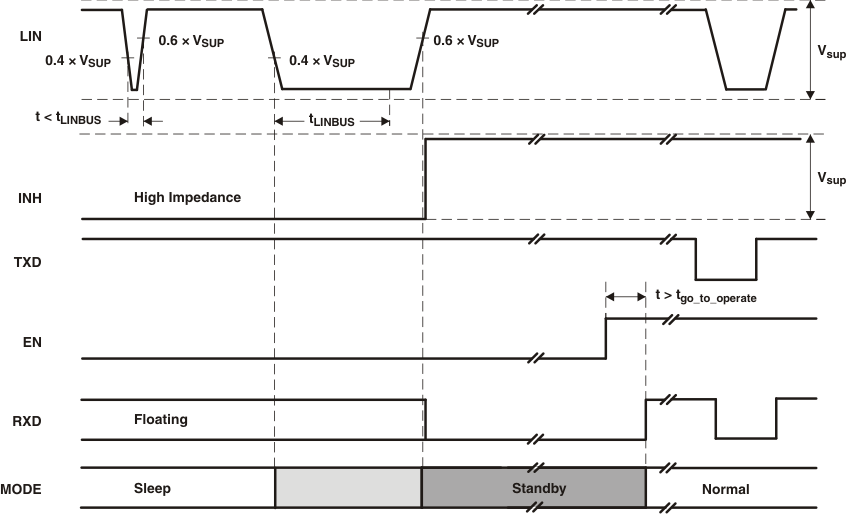
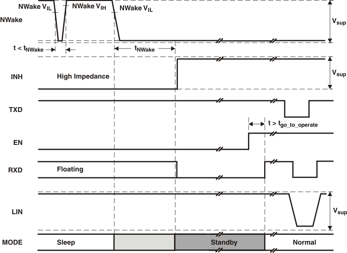
This mode is entered whenever a wake-up event occurs through LIN bus or NWake while the TPIC1021A is in sleep mode. The LIN bus responder termination circuit and INH are turned on when standby mode is entered. The application system powers up once INH is turned on, assuming the system is using a voltage regulator connected through INH. Standby mode is signaled through a low level on RXD.

When EN is set high while the TPIC1021A is in standby mode the device returns to normal mode and the normal transmission paths from TXD to LIN bus and LIN bus to RXD are enabled.
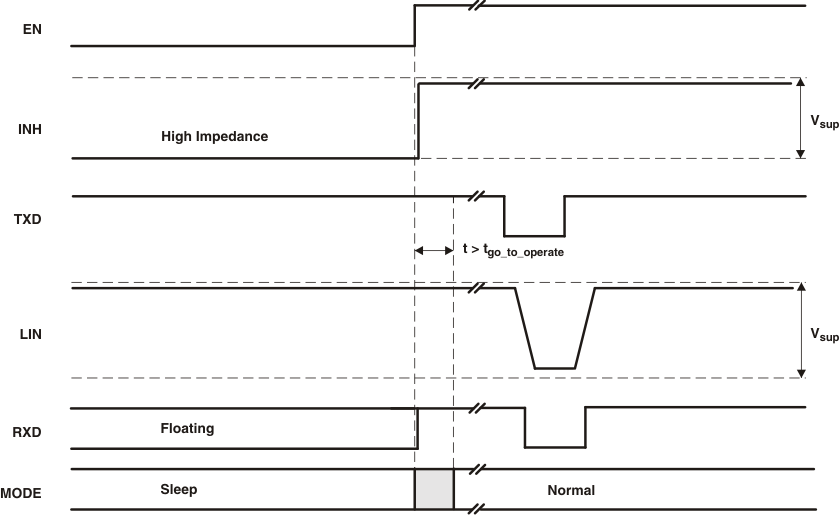
GUID-A3AA1160-4565-4E7C-8207-CADB4965E0BF-low.gifFigure 10-2 Wakeup Through EN
GUID-912714A8-978D-42D8-B4FF-A3FCA5860FE8-low.gifFigure 10-3 Wakeup Through LIN
GUID-001D9572-BCC4-445A-810F-F4B1EC4662F4-low.gifFigure 10-4 Wakeup Through NWake