SLIS061D July 1998 – September 2015 TPIC6C595
PRODUCTION DATA.
- 1 Features
- 2 Applications
- 3 Description
- 4 Revision History
- 5 Pin Configuration and Functions
- 6 Specifications
- 7 Parameter Measurement Information
- 8 Detailed Description
- 9 Application and Implementation
- 10Power Supply Recommendations
- 11Layout
- 12Device and Documentation Support
- 13Mechanical, Packaging, and Orderable Information
Package Options
Refer to the PDF data sheet for device specific package drawings
Mechanical Data (Package|Pins)
- PW|16
- |
- N|16
- D|16
Thermal pad, mechanical data (Package|Pins)
Orderable Information
9 Application and Implementation
NOTE
Information in the following applications sections is not part of the TI component specification, and TI does not warrant its accuracy or completeness. TI’s customers are responsible for determining suitability of components for their purposes. Customers should validate and test their design implementation to confirm system functionality.
9.1 Application Information
The TPIC6C595 is a serial-in parallel-out, Power+LogicE 8-bit shift register with low-side switch DMOS outputs rating of 100 mA per channel. The device is designed for use in systems that require relatively moderate load power such as LEDs. The device contains a built-in voltage clamp on the outputs for inductive transient protection. Power driver applications include relays, solenoids, and other low current or medium-voltage loads. The following focuses on automotive cluster applications for the TPIC6C595.
9.2 Typical Application
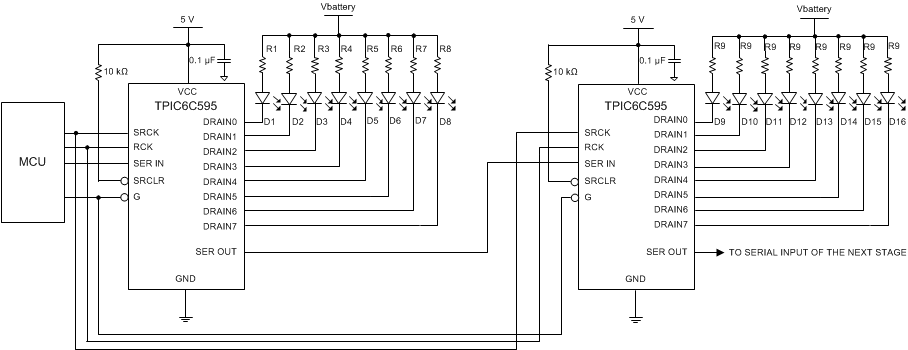
The typical application of TPIC6C595 is automotive cluster driver. In this example, two TPIC6C595 power shift registers are cascaded and used to turn on LEDs in the cluster panel. In this case, the LED must be updated after all 16 bits of data have been loaded into the serial shift registers. MCU outputs the data to the serial input (SER IN) while clocking the shift register clock (SRCK). After the 16th clock, a pulse to the register clock (RCK) transfers the data to the storage registers. If output enable (G) is low, then the LEDs are turned on corresponding to the status word with ones being on and zeros off. With this simple scheme, MCU can use the SPI interface to turn on 16 LEDs using only two ICs as illustrated in Figure 14.
 Figure 14. Typical Application Schematic
9.2.1 Design Requirements
Table 1 shows the design parameters for this typical application.
Table 1. Design Parameters
| DESIGN PARAMETERS | EXAMPLE VALUE |
|---|---|
| Vsupply | 9 V to 16 V |
| V(D1), V(D2), V(D3), V(D4), V(D5), V(D6),V(D7), V(D8) | 2 V |
| V(D9), V(D10),V(D11), V(D12), V(D13), V(D14),V(D15), V(D16) | 3.3 V |
| I(D1), I(D2), I(D3), I(D4), I(D5), I(D6),I(D7), I(D8) | 20 mA when Vbattery is 12 V |
| I(D9), I(D10), I(D11), I(D12), I(D13), I(D14),I(D15), I(D16) | 30 mA when Vbattery is 12 V |
9.2.2 Detailed Design Procedure
9.2.2.1 Step-by-Step Design Procedure
To begin the design process, one must decide on a few parameters. The designer must know the following:
- Vsupply – LED supply is connected directly to the car battery, which has a voltage range from 9 V to 16 V, or fixed voltage. This application connects to the battery directly.
- V(Dx) – LED forward voltage
- I(Dx) – LED setting current when battery is 12 V.
9.2.2.1.1 R1, R2, R3, R4, R5, R6, R7, R8
When Vsupply is 9 V, I(D1) = I(D2) = I(D3) = I(D4) = I(D5) = I(D6) = I(D7) = I(D8) = (Vsupply – V(Dx)) / Rx = 14 mA.
When Vsupply is 16 V, I(D1) = I(D2) = I(D3) = I(D4) = I(D5) = I(D6) = I(D7) = I(D8) = (Vsupply – V(Dx)) / Rx = 28 mA.
9.2.2.1.2 R9, R10, R11, R12, R13, R14, R15, R16
When Vsupply is 9 V, I(D9) = I(D10) = I(D11) = I(D12) = I(D13) = I(D14) = I(D15) = I(D16) = (Vsupply – V(Dx)) / Rx = 19.7 mA.
When Vsupply is 16 V, I(D9) = I(D10) = I(D11) = I(D12) = I(D13) = I(D14) = I(D15) = I(D16) = (Vsupply – V(Dx)) / Rx = 43.8 mA.
NOTE
If customer can accept the current variation when battery voltage is changing, they can connect to battery directly. If customer needs the less variation of current, they must use the voltage regulator as supply voltage of LED, or change to constant current LED driver directly.
9.2.3 Application Curve
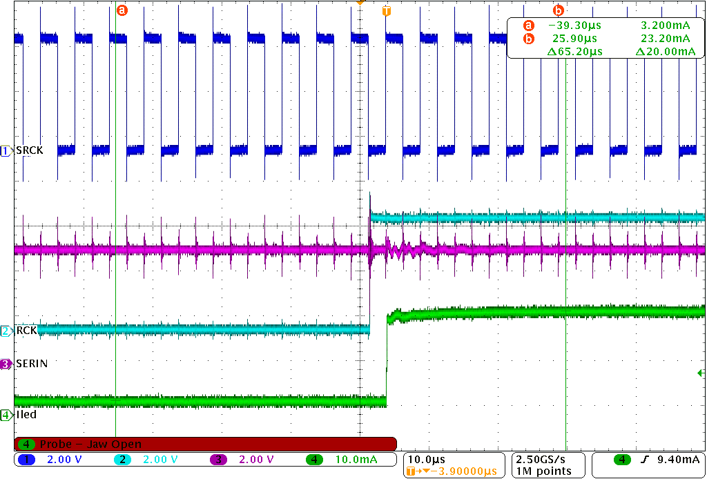
 Figure 15. CH1 is SRCK, CH2 is RCK, CH3 is SERIN, CH4 is D1 current